KS8993F Micrel Inc, KS8993F Datasheet - Page 8
KS8993F
Manufacturer Part Number
KS8993F
Description
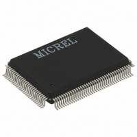
IC CONV MED 10/100 3PORT 128PQFP
Manufacturer
Micrel Inc
Datasheet
1.KS8993F.pdf
(100 pages)
Specifications of KS8993F
Applications
*
Mounting Type
Surface Mount
Package / Case
128-MQFP, 128-PQFP
Number Of Primary Switch Ports
3
Internal Memory Buffer Size
32
Operating Supply Voltage (typ)
1.8/2.5/3.3V
Fiber Support
Yes
Integrated Led Drivers
Yes
Phy/transceiver Interface
MII/SNI
Power Supply Type
Analog/Digital
Package Type
PQFP
Data Rate (typ)
10/100Mbps
Vlan Support
Yes
Operating Temperature (max)
70C
Operating Temperature (min)
0C
Pin Count
128
Mounting
Surface Mount
Jtag Support
No
Operating Supply Voltage (max)
1.89/3.465V
Operating Temperature Classification
Commercial
Lead Free Status / RoHS Status
Lead free / RoHS Compliant
For Use With
KS8993F-EVAL - EVAL KIT EXPERIMENTAL KS8993F
Lead Free Status / RoHS Status
Not Compliant, Lead free / RoHS Compliant
Available stocks
Company
Part Number
Manufacturer
Quantity
Price

Part Number:
KS8993FA5
Manufacturer:
MICREL/麦瑞
Quantity:
20 000
Part Number:
KS8993FL
Manufacturer:
MICREL/麦瑞
Quantity:
20 000


Table 1: FX and TX Mode Selection.................................................................................................................................................. 26
Table 2: MDI/MDI-X Pin Definition..................................................................................................................................................... 27
Table 3: MII Signals........................................................................................................................................................................... 35
Table 4: SNI (7-wire) Signals............................................................................................................................................................. 35
Table 5: MII Management Interface frame format ............................................................................................................................. 36
Table 6: Serial Management Interface (SMI) frame format ............................................................................................................... 37
Table 7: FID+DA look up in VLAN mode........................................................................................................................................... 39
Table 8: FID+SA look up in VLAN mode ........................................................................................................................................... 39
Table 9: KS8993F SPI Connections.................................................................................................................................................. 44
Table 10: Format of Static MAC Table (8 entries) ............................................................................................................................. 79
Table 11: Format of Static VLAN Table (16 entries).......................................................................................................................... 80
Table 12: Format of Dynamic MAC Table (1K entries)...................................................................................................................... 81
Table 13: Format of “Per Port” MIB Counters.................................................................................................................................... 82
Table 14: Port 1’s “Per Port” MIB Counters Indirect Memory Offsets................................................................................................ 82
Table 15: Format of “All Port Dropped Packet” MIB Counters .......................................................................................................... 84
Table 16: “All Port Dropped Packet” MIB Counters Indirect Memory Offsets.................................................................................... 84
Table 17: EEPROM Timing Parameters............................................................................................................................................ 89
Table 18: SNI Timing Parameters ..................................................................................................................................................... 90
Table 19: MAC mode MII Timing Parameters ................................................................................................................................... 91
Table 20: PHY Mode MII Timing Parameters .................................................................................................................................... 92
Table 21: SPI Input Timing Parameters ............................................................................................................................................ 93
Table 22: SPI Output Timing Parameters.......................................................................................................................................... 94
Table 23: Reset Timing Parameters.................................................................................................................................................. 97
Table 24: Transformer Selection Criteria........................................................................................................................................... 99
Table 25: Qualified Single Port Magnetic .......................................................................................................................................... 99
Table 26: Crystal/Oscillator Selection Criteria ................................................................................................................................... 99
Figure 1: Typical Straight Cable Connection ..................................................................................................................................... 28
Figure 2: Typical Crossover Cable Connection ................................................................................................................................. 28
Figure 3: Auto Negotiation and Parallel Detection ............................................................................................................................ 29
Figure 4: Destination Address look up flowchart, stage 1 ................................................................................................................. 31
Figure 5: Destination Address resolution flowchart, stage 2 ............................................................................................................. 32
Figure 6: 802.1p Priority Field Format............................................................................................................................................... 40
Figure 7: KS8993F EEPROM Configuration Timing Diagram ........................................................................................................... 42
Figure 8: SPI Write Data Cycle ......................................................................................................................................................... 45
Figure 9: SPI Read Data Cycle ......................................................................................................................................................... 45
Figure 10: SPI Multiple Write............................................................................................................................................................. 46
Figure 11: SPI Multiple Read............................................................................................................................................................. 46
Figure 12: EEPROM Interface Input Timing Diagram ....................................................................................................................... 89
Figure 13: EEPROM Interface Output Timing Diagram..................................................................................................................... 89
Figure 14: SNI Input Timing Diagram ................................................................................................................................................ 90
Figure 15: SNI Output Timing Diagram ............................................................................................................................................. 90
Figure 16: MAC Mode MII Timing - Data received from MII .............................................................................................................. 91
Figure 17: MAC Mode MII Timing - Data transmitted to MII .............................................................................................................. 91
Figure 18: PHY Mode MII Timing – Data received from MII .............................................................................................................. 92
Figure 19: PHY Mode MII Timing - Data transmitted to MII............................................................................................................... 92
Figure 20: SPI Input Timing............................................................................................................................................................... 93
Figure 21: SPI Output Timing ............................................................................................................................................................ 94
Figure 22: MDC/MDIO Timing for MIIM and SMI Interfaces .............................................................................................................. 95
Figure 23: Auto Negotiation Timing................................................................................................................................................... 96
Figure 24: Reset Timing .................................................................................................................................................................... 97
Figure 25: Recommended Reset Circuit ........................................................................................................................................... 98
Figure 26: Recommended Reset Circuit for interfacing with CPU/FPGA Reset Output.................................................................... 98
Figure 27: 128-pin PQFP Package Outline Drawing ....................................................................................................................... 100
Micrel, Inc.
June 2009
List of Figures
List of Tables
8
hbwhelp@micrel.com
or (408) 955-1690
M9999-062509
KS8993F/FL
Related parts for KS8993F
Image
Part Number
Description
Manufacturer
Datasheet
Request
R

Part Number:
Description:
Manufacturer:
Micrel Inc
Datasheet:
Part Number:
Description:
Manufacturer:
Micrel Inc
Datasheet:
Part Number:
Description:
Manufacturer:
Micrel Inc
Datasheet:
Part Number:
Description:
Manufacturer:
Micrel Inc
Datasheet:
Part Number:
Description:
Manufacturer:
Micrel Inc
Datasheet:
Part Number:
Description:
Manufacturer:
Micrel Inc
Datasheet:
Part Number:
Description:
Manufacturer:
Micrel Inc
Datasheet:
Part Number:
Description:
Manufacturer:
Micrel Inc
Datasheet:
Part Number:
Description:
Manufacturer:
Micrel Inc
Datasheet:
Part Number:
Description:
Manufacturer:
Micrel Inc
Datasheet:
Part Number:
Description:
Manufacturer:
Micrel Inc
Datasheet:
Part Number:
Description:
Manufacturer:
Micrel Inc
Datasheet:
Part Number:
Description:
Manufacturer:
Micrel Inc
Datasheet:
Part Number:
Description:
Manufacturer:
Micrel Inc
Datasheet: