AFBR-5805Z Avago Technologies US Inc., AFBR-5805Z Datasheet - Page 7
AFBR-5805Z
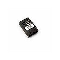
Manufacturer Part Number
AFBR-5805Z
Description
TXRX ATM SONET OC3 3V SC 1X9
Manufacturer
Avago Technologies US Inc.
Series
-r
Specifications of AFBR-5805Z
Wavelength
1310nm
Applications
General Purpose
Voltage - Supply
3.3V
Connector Type
SC
Mounting Type
Through Hole
Function
Provides the system designer with products to implement a range of soluntions for multimode fiber SONET OC-3 (SDH STM-1)
Product
Transceiver
Data Rate
155 Mbps
Maximum Rise Time
3 ns/2.2 ns
Maximum Fall Time
3 ns/2.2 ns
Pulse Width Distortion
1.2 ns (Max)/1.91 ns (Max)
Maximum Output Current
50 mA
Operating Supply Voltage
3.135 V to 3.5 V or 4.75 V to 5.25 V
Maximum Operating Temperature
+ 70 C
Minimum Operating Temperature
0 C
Package / Case
SIP-9
Lead Free Status / RoHS Status
Lead free / RoHS Compliant
For Use With
Multimode Glass
Lead Free Status / RoHS Status
Lead free / RoHS Compliant, Lead free / RoHS Compliant
Available stocks
Company
Part Number
Manufacturer
Quantity
Price
Company:

Part Number:
AFBR-5805Z
Manufacturer:
Avago Technologies
Quantity:
135


Recommended Handling Precautions
Avago Technologies recommends that normal static pre-
cautions be taken in the handling and assembly of these
transceivers to prevent damage which may be induced
by electrostatic discharge (ESD). The AFBR-5800Z series
of transceivers meet MIL-STD-883C Method 3015.4 Class
2 products.
Care should be used to avoid shorting the receiver data or
signal detect outputs directly to ground without proper
current limiting impedance.
Solder and Wash Process Compatibility
The transceivers are delivered with protective process
plugs inserted into the duplex SC or duplex ST connector
receptacle. This process plug protects the optical subas-
semblies during wave solder and aqueous wash process-
ing and acts as a dust cover during shipping.
These transceivers are compat ible with either industry
standard wave or hand solder processes.
7
NOTES:
THE SPLIT-LOAD TERMINATIONS FOR ECL SIGNALS NEED TO BE LOCATED AT THE INPUT
R1 = R4 = R6 = R8 = R10 = 130 OHMS FOR +5.0 V OPERATION, 82 OHMS FOR +3.3 V OPERATION.
R2 = R3 = R5 = R7 = R9 = 82 OHMS FOR +5.0 V OPERATION, 130 OHMS FOR +3.3 V OPERATION.
C1 = C2 = C3 = C5 = C6 = 0.1 µF.
C4 = 10 µF.
L1 = L2 = 1 µH COIL OR FERRITE INDUCTOR.
Figure 7. Recommended Decoupling and Termination Circuits
TERMINATION
AT PHY
DEVICE
INPUTS
OF DEVICES RECEIVING THOSE ECL SIGNALS. RECOMMEND 4-LAYER PRINTED CIRCUIT
BOARD WITH 50 OHM MICROSTRIP SIGNAL PATHS BE USED.
NO INTERNAL CONNECTION
V
Rx
EE
R6
1
RD
R5
RD
2
V
CC
C6
RD
R7
RD
3
R8
Rx
SD
SD
4
AFBR-5805Z
TOP VIEW
R10
R9
C1
TRANSCEIVER
V
AT V
Rx
C3
CC
V
5
CC
L1
V
FILTER
CC
CC
PINS
NO INTERNAL CONNECTION
V
Tx
CC
6
C4
L2
Tx
C2
TD
7
TD
TERMINATION
AT TRANSCEIVER
INPUTS
R1
TD
R2
8
V
CC
V
Tx
C5
R3
EE
9
R4
TD
Shipping Container
The transceiver is packaged in a shipping container de-
signed to protect it from mechanical and ESD damage
during shipment or storage.
Board Layout - Decoupling Circuit and Ground Planes
It is important to take care in the layout of your circuit
board to achieve optimum perform ance from these trans-
ceivers. Figure 7 provides a good example of a schematic
for a power supply decoupling circuit that works well
with these parts. It is further recommended that a con-
tiguous ground plane be provided in the circuit board di-
rectly under the transceiver to provide a low inductance
ground for signal return current. This recommen da tion is
in keeping with good high frequency board layout prac-
tices.
Related parts for AFBR-5805Z
Image
Part Number
Description
Manufacturer
Datasheet
Request
R

Part Number:
Description:
650nm FE Transceiver Eval Kit
Manufacturer:
Avago Technologies US Inc.
Datasheet:

Part Number:
Description:
TXRX OPT OC3 MTRJ SFF 2X5DIP
Manufacturer:
Avago Technologies US Inc.
Datasheet:

Part Number:
Description:
TXRX ETHERNET 125MBD MMF 2X5
Manufacturer:
Avago Technologies US Inc.
Datasheet:

Part Number:
Description:
TXRX OPT SFP DGTL 850NM IND
Manufacturer:
Avago Technologies US Inc.
Datasheet:

Part Number:
Description:
TXRX OPT SFF 4/2/1GBD 2X7
Manufacturer:
Avago Technologies US Inc.
Datasheet:

Part Number:
Description:
TXRX OPT SFP 4/2/1GBD 850NM
Manufacturer:
Avago Technologies US Inc.
Datasheet:

Part Number:
Description:
TXRX OPT XFP 10GB/S 850NM
Manufacturer:
Avago Technologies US Inc.
Datasheet:

Part Number:
Description:
TXRX OPT 1X9 100MBPS ST EXT TEMP
Manufacturer:
Avago Technologies US Inc.
Datasheet:

Part Number:
Description:
TXRX OPT 1X9 100MBPS SC EXT TEMP
Manufacturer:
Avago Technologies US Inc.
Datasheet:

Part Number:
Description:
TXRX OPT 1X9 100MBPS DUPLEX SC
Manufacturer:
Avago Technologies US Inc.
Datasheet:

Part Number:
Description:
OPTOCOUPLER GATE DRV 2A 16-SOIC
Manufacturer:
Avago Technologies US Inc.
Datasheet:
Part Number:
Description:
OPTOCOUPLER 2CH 2.5A 16-SOIC
Manufacturer:
Avago Technologies US Inc.
Datasheet:

Part Number:
Description:
OPTOCOUPLER GATE DRV 0.4A 16SOIC
Manufacturer:
Avago Technologies US Inc.
Datasheet:

Part Number:
Description:
OPTOCOUPLER 2.0A 250KHZ 8-DIP
Manufacturer:
Avago Technologies US Inc.
Datasheet:

Part Number:
Description:
OPTOCOUPLER 2.0A 250KHZ GW 8-SMD
Manufacturer:
Avago Technologies US Inc.
Datasheet: