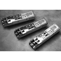
AFBR-59M5LZ Avago Technologies US Inc., AFBR-59M5LZ Datasheet - Page 7

AFBR-59M5LZ
Manufacturer Part Number
AFBR-59M5LZ
Description
TXRX OPT 850NM SFF 2X6
Manufacturer
Avago Technologies US Inc.
Datasheet
1.AFBR-59M5LZ.pdf
(18 pages)
Specifications of AFBR-59M5LZ
Applications
Ethernet
Data Rate
2.215Gbd
Wavelength
850nm
Voltage - Supply
2.97 V ~ 3.63 V
Connector Type
LC Duplex
Mounting Type
Through Hole
Data Rate Max
2.125Gbps
Supply Voltage
3.3V
Wavelength Typ
850nm
Leaded Process Compatible
Yes
Lead Free Status / RoHS Status
Lead free / RoHS Compliant
Table 2. Pin Description
Notes:
1. TX_DISABLE is an input that is used to shut down the transmitter optical output. It is pulled down with 6.8 k: internal to the transceiver.
2. The signals SDA and SCL designate the two wire serial interface pins. They must be pulled up with a 4.7 k – 10 k: resistor on the host board. SCL
3. Signal Detect is a normally high LVTTL output. When high it indicates the received optical power is adequate for normal operation. When Low, it
4. RD-/+ designate the differential receiver outputs. They are ac coupled 100 : differential lines which should be terminated with 100 : differential
5. V
6. TD-/+ designate the differential transmitter inputs. They are ac coupled differential lines with 100 : differential termination inside the module. The
7. Transmitter and Receiver Ground are common internally on the transceiver PCB. They are electrically connected to signal ground within the
7
Pin
1
2
3
4
5
6
7
8
9
10
A
B
Low (0 – 0.8 V) or Open:
Between (0.8 V and 2.0 V):
High (2.0 – V
The TX_DISABLE pin state is logic Or’d with the contents of EEPROM address A2h, byte 110 bit 6 (soft disable control bit) to control the transmit
output.
is the serial clock line of two wire serial interface. SDA is the serial data line of two wire serial interface
indicates the received optical power is insufficient to guarantee error free operation. In the low state, the output will be pulled to < 0.8 V.
at the host SerDes input. AC coupling is done inside the transceiver and is not required on the host board. The voltage swing on these lines will be
between 600 and 1600 mV differential (300 – 800 mV single ended) when properly terminated.
ac coupling is done inside the module and is not required on the host board. The inputs will accept differential swings of 400 – 2400 mV (200 – 1200
mV single ended), though it is recommended that values between 500 and 1200 mV differential (250 – 600 mV single ended) be used for best EMI
performance.
transceiver.
CC
R and V
Name
V
V
SD
RD-
RD+
V
V
TX_DISABLE
TD+
TD-
SDA
SCL
EE
CC
CC
EE
R
T
R
T
CC
CC
T are the receiver and transmitter power supplies. They are defined at the transceiver pins.
max):
Function/Description
Receiver Signal Ground
Receiver Power Supply: +3.3V
TTL Signal Detect: Active High
Received Data Out Bar
Received Data Out
Transmitter Power Supply: +3.3V
Transmitter Signal Ground
TTL Transmitter Disable: Active High,
(Open = Enabled)
Transmitter Data In
Transmitter Data In Bar
Serial Interface Data I/O (Mod-def2)
Serial Interface Clock Input (Mod-def1)
Transmitter Enabled
Undefined
Transmitter Disabled
Notes
7
5
3
4
4
5
7
1
6
6
2
2
Figure 4. Module pin configuration.
10
6
7
8
9
B
TOP VIEW
5
4
3
2
1
A


