AFCT-5805DZ Avago Technologies US Inc., AFCT-5805DZ Datasheet - Page 3
AFCT-5805DZ
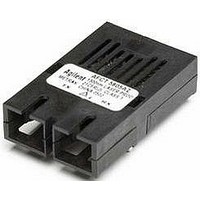
Manufacturer Part Number
AFCT-5805DZ
Description
TXRX OPT SM 155MBS SONET OC3/SDH
Manufacturer
Avago Technologies US Inc.
Datasheet
1.AFCT-5805BZ.pdf
(10 pages)
Specifications of AFCT-5805DZ
Applications
General Purpose
Data Rate
155Mbps
Wavelength
1300nm
Voltage - Supply
*
Connector Type
SC
Mounting Type
Through Hole
Data Rate Max
0.155Gbps
Supply Voltage
5V
Wavelength Typ
1300nm
Peak Reflow Compatible (260 C)
Yes
Optical Fiber Type
TX/RX
Data Transfer Rate
155Mbps
Optical Rise Time
2/2.2ns
Optical Fall Time
2/2.2ns
Operating Temperature Classification
Commercial
Peak Wavelength
1360nm
Operating Supply Voltage (min)
3.1V
Operating Supply Voltage (typ)
3.3/5V
Operating Supply Voltage (max)
5.25V
Operating Temp Range
0C to 70C
Mounting
Through Hole
Pin Count
9
Lead Free Status / RoHS Status
Lead free / RoHS Compliant
Lead Free Status / RoHS Status
Lead free / RoHS Compliant, Lead free / RoHS Compliant
Available stocks
Company
Part Number
Manufacturer
Quantity
Price

Part Number:
AFCT-5805DZ
Manufacturer:
AVAGO/安华高
Quantity:
20 000


Recommended Circuit Schematic
In order to ensure proper functionality of the AFCT-
5805xxZ a recommended circuit is provided in Figure
3. When designing the circuit interface, there are a few
fundamental guidelines to follow. For example, in the Rec-
ommended Circuit Schematic figure the differential data
lines should be treated as 50 ohm Microstrip or stripline
transmission lines. This will help to minimize the parasitic
inductance and capacitance effects. Proper termination
of the differential data signals will prevent reflections and
ringing which would compromise the signal fidelity and
generate unwanted electrical noise. Locate termination
at the received signal end of the transmission line. The
length of these lines should be kept short and of equal
length. For the high speed signal lines, differential sig-
nals should be used, not single-ended signals, and these
differential signals need to be loaded symmetrically to
prevent unbalanced currents from flowing which will
cause distortion in the signal.
Maintain a solid, low inductance ground plane for re-
turning signal currents to the power supply. Multilayer
plane printed circuit board is best for distribution of V
returning ground currents, forming transmission lines
and shielding, Also, it is important to suppress noise from
influencing the fiber-optic transceiver performance, es-
pecially the receiver circuit. Proper power supply filtering
of V
Figure 3. Recommended Circuit Schematic
3
TERMINATE
AT PHY
DEVICE
INPUTS
CC
for this transceiver is accomplished by using the
R6
NO INTERNAL
CONNECTION
V
Rx
EER
1
RD
R5
V
RD
CC
C6
2
RD
R7
RD
3
R8
SD
R10
SD
4
C1
TOP VIEW
C3
TRANSCEIVER
C7
AT V
V
V
R9
Rx
CCR
5
cc
L1 L2
FILTER
V
cc
CC
PINS
V
Tx
CCT
6
C2
C4
C8
TD
7
TD
NO INTERNAL
CONNECTION
TERMINATION
TRANSCEIVER
R1
TD
R2
8
INPUTS
V
CC
C5
AT
V
R3
Tx
CC
EET
9
,
R4
TD
recommended, separate filter circuits shown in Figure
3 for the transmitter and receiver sections. These filter
circuits suppress V
this prevents receiver sensitivity degradation due to V
noise. It is recommended that surface-mount compo-
nents be used. Use tantalum capacitors for the 10 µF
capacitors and monolithic, ceramic bypass capacitors for
the 0.1 µF capacitors. Also, it is recommended that a sur-
face- mount coil inductor of 3.3 µH be used. Ferrite beads
can be used to replace the coil inductors when using
quieter V
over a ferrite bead. All power supply components need to
be placed physically next to the V
and transmitter. Use a good, uniform ground plane with
a minimum number of holes to provide a low-inductance
ground current return for the power supply currents.
In addition to these recommendations, Avago Tech-
nologies Application Engineering staff is available for
consulting on best layout practices with various vendors
mux/demux, clock generator and clock recovery circuits.
Avago Technologies has participated in several reference
design studies and is prepared to share the findings of
these studies with interested customers. Contact your
local Avago Technologies sales representative to arrange
for this service.
NOTES:
THE SPLIT-LOAD TERMINATIONS FOR PECL SIG-
NALS NEED TO BE LOCATED AT THE INPUT OF
DEVICES RECEIVING THOSE PECL SIGNALS.
RECOMMEND 4-LAYER PRINTED CIRCUIT BOARD
WITH 50 Ω MICROSTRIP SIGNAL PATHS BE USED.
R1 = R4 = R6 = R8 = R10 = 130 Ω FOR +5.0V OP-
ERATION, 82 Ω FOR +3.3V OPERATION.
R2 = R3 = R5 = R7 = R9 = 82 Ω FOR +5.0V OPERA-
TION, 130 Ω FOR +3.3V OPERATION.
C1 = C2 = 10 µF
C3 = C4 = C7 = C8 = 100 nF
C5 = C6 = 0.1 µF
L1 = L2 = 3.3 µH COIL OR FERRITE INDUCTOR.
CC
supplies, but a coil inductor is recommended
CC
noise over a broad frequency range,
CC
pins of the receiver
CC
Related parts for AFCT-5805DZ
Image
Part Number
Description
Manufacturer
Datasheet
Request
R

Part Number:
Description:
TXRX OPT 1X9 155MB/S 1300NM BK
Manufacturer:
Avago Technologies US Inc.
Datasheet:

Part Number:
Description:
TXRX OPT SFF PLUGGABLE BAIL
Manufacturer:
Avago Technologies US Inc.
Datasheet:
Part Number:
Description:
TXRX OPT SFF PLUGGABLE BAIL DMI
Manufacturer:
Avago Technologies US Inc.
Datasheet:

Part Number:
Description:
TXRX 125MBD DUPLEX BLACK SC 1X9
Manufacturer:
Avago Technologies US Inc.
Datasheet:
Part Number:
Description:
TXRX 125MBD DUPLEX BLUE SC 1X9
Manufacturer:
Avago Technologies US Inc.
Datasheet:
Part Number:
Description:
TXRX SFF SM OC3/STM-1 BAIL DMI
Manufacturer:
Avago Technologies US Inc.
Datasheet:
Part Number:
Description:
TXRX 125MBD DUPLEX BLACK SC 1X9
Manufacturer:
Avago Technologies US Inc.
Datasheet:
Part Number:
Description:
TXRX 125MBD DUPLEX BLUE SC 1X9
Manufacturer:
Avago Technologies US Inc.
Datasheet:

Part Number:
Description:
TXRX OPT SM 155MBS SONET OC3/SDH
Manufacturer:
Avago Technologies US Inc.
Datasheet:

Part Number:
Description:
TXRX OPT SM 155MBS SONET OC3/SDH
Manufacturer:
Avago Technologies US Inc.
Datasheet:

Part Number:
Description:
OPTOCOUPLER GATE DRV 2A 16-SOIC
Manufacturer:
Avago Technologies US Inc.
Datasheet:
Part Number:
Description:
OPTOCOUPLER 2CH 2.5A 16-SOIC
Manufacturer:
Avago Technologies US Inc.
Datasheet:

Part Number:
Description:
OPTOCOUPLER GATE DRV 0.4A 16SOIC
Manufacturer:
Avago Technologies US Inc.
Datasheet:

Part Number:
Description:
OPTOCOUPLER 2.0A 250KHZ 8-DIP
Manufacturer:
Avago Technologies US Inc.
Datasheet:

Part Number:
Description:
OPTOCOUPLER 2.0A 250KHZ GW 8-SMD
Manufacturer:
Avago Technologies US Inc.
Datasheet: