AFCT-5971ALZ Avago Technologies US Inc., AFCT-5971ALZ Datasheet - Page 6
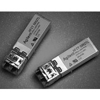
AFCT-5971ALZ
Manufacturer Part Number
AFCT-5971ALZ
Description
TXRX FE SM LASER 125MBS 2X5
Manufacturer
Avago Technologies US Inc.
Datasheet
1.AFCT-5971LZ.pdf
(15 pages)
Specifications of AFCT-5971ALZ
Applications
Ethernet
Data Rate
125MBd
Wavelength
1300nm
Voltage - Supply
3.1 V ~ 3.5 V
Connector Type
LC Duplex
Mounting Type
Through Hole
Data Rate Max
0.125Gbps
Supply Voltage
3.3V
Wavelength Typ
1300nm
Leaded Process Compatible
Yes
Optical Fiber Type
TX/RX
Data Transfer Rate
155Mbps
Optical Rise Time
2/2.2ns
Optical Fall Time
2/2.2ns
Operating Temperature Classification
Industrial
Peak Wavelength
1360/1580nm
Package Type
DIP With Connector
Operating Supply Voltage (min)
3.1V
Operating Supply Voltage (typ)
3.3V
Operating Supply Voltage (max)
3.5V
Output Current
50mA
Operating Temp Range
-40C to 85C
Mounting
Snap Fit To Panel
Pin Count
10
Product
Transceiver
Maximum Rise Time
2 ns, 2.2 ns
Maximum Fall Time
2 ns, 2.2 ns
Maximum Output Current
50 mA
Operating Supply Voltage
3.1 V to 3.5 V
Maximum Operating Temperature
+ 85 C
Minimum Operating Temperature
- 40 C
Package / Case
DIP-10 with Connector
Function
Applications specified for signal rate of 125 MBd, for Fast Ethernet, and Singlemode Fiber.
Lead Free Status / RoHS Status
Lead free / RoHS Compliant
For Use With
Singlemode Glass
Lead Free Status / RoHS Status
Lead free / RoHS Compliant, Lead free / RoHS Compliant
Available stocks
Company
Part Number
Manufacturer
Quantity
Price
Company:

Part Number:
AFCT-5971ALZ
Manufacturer:
Avago Technologies
Quantity:
135


Connection Diagram
Figure 5. Pin Out Diagram (Top View)
Pin Descriptions:
Pin 1 Receiver Signal Ground V
Directly connect this pin to the receiver ground plane.
Pin 2 Receiver Power Supply V
Provide +3.3 V dc via the recommended receiver power
supply filter circuit. Locate the power supply filter cir-
cuit as close as possible to the V
circuit should not cause V
specification.
Pin 3 Signal Detect SD:
Normal optical input levels to the receiver result in a
logic “1” output.
Low optical input levels to the receiver result in a logic
“0” output.
This Signal Detect output can be used to drive a LVPECL
input on an upstream circuit, such as Signal Detect in-
put or Loss of Signal-bar.
Pin 4 Receiver Data Out Bar RD-:
No internal terminations are provided. See recommend-
ed circuit schematic.
Pin 5 Receiver Data Out RD+:
No internal terminations are provided. See recommend-
ed circuit schematic.
RECEIVER SIGNAL GROUND
RECEIVER POWER SUPPLY
RECEIVER DATA OUT BAR
RECEIVER DATA OUT
SIGNAL DETECT
o
o
o
o
o
CC
RX
CC
EE
1
2
3
4
5
RX:
to drop below minimum
View
RX:
Top
CC
RX pin. Note: the filter
10
TX
9
8
7
6
o
o
o
o
o
TRANSMITTER DATA IN BAR
TRANSMITTER DATA IN
TRANSMITTER DISABLE
TRANSMITTER SIGNAL GROUND
TRANSMITTER POWER SUPPLY
Mounting Studs/
Solder Posts
Pin 6 Transmitter Power Supply
V
Provide +3.3 V dc via the recommended transmitter
power supply filter circuit. Locate the power supply fil-
ter circuit as close as possible to the V
Pin 7 Transmitter Signal Ground
V
Directly connect these pins to the transmitter signal
ground plane.
Pin 8 Transmitter Disable T
Optional feature, connect this pin to +3.3 V TTL logic
high “1” to disable module. To enable module connect to
TTL logic low “0”.
Pin 9 Transmitter Data In TD+:
No internal terminations are provided. See recommend-
ed circuit schematic.
Pin 10 Transmitter Data In Bar TD-:
No internal terminations are provided. See recommend-
ed circuit schematic.
Mounting Studs/Solder Posts
The two mounting studs are provided for transceiver
mechanical attachment to the circuit board. It is rec-
ommended that the holes in the circuit board be con-
nected to chassis ground.
CC
EE
TX:
TX:
DIS
:
CC
TX pin.
Related parts for AFCT-5971ALZ
Image
Part Number
Description
Manufacturer
Datasheet
Request
R

Part Number:
Description:
TXRX OPT 1X9 155MB/S 1300NM BK
Manufacturer:
Avago Technologies US Inc.
Datasheet:

Part Number:
Description:
TXRX OPT SFF PLUGGABLE BAIL
Manufacturer:
Avago Technologies US Inc.
Datasheet:
Part Number:
Description:
TXRX OPT SFF PLUGGABLE BAIL DMI
Manufacturer:
Avago Technologies US Inc.
Datasheet:

Part Number:
Description:
TXRX 125MBD DUPLEX BLACK SC 1X9
Manufacturer:
Avago Technologies US Inc.
Datasheet:
Part Number:
Description:
TXRX 125MBD DUPLEX BLUE SC 1X9
Manufacturer:
Avago Technologies US Inc.
Datasheet:

Part Number:
Description:
TXRX OPT SM 155MBS SONET OC3/SDH
Manufacturer:
Avago Technologies US Inc.
Datasheet:
Part Number:
Description:
TXRX SFF SM OC3/STM-1 BAIL DMI
Manufacturer:
Avago Technologies US Inc.
Datasheet:
Part Number:
Description:
TXRX 125MBD DUPLEX BLACK SC 1X9
Manufacturer:
Avago Technologies US Inc.
Datasheet:
Part Number:
Description:
TXRX 125MBD DUPLEX BLUE SC 1X9
Manufacturer:
Avago Technologies US Inc.
Datasheet:

Part Number:
Description:
TXRX OPT SM 155MBS SONET OC3/SDH
Manufacturer:
Avago Technologies US Inc.
Datasheet:

Part Number:
Description:
OPTOCOUPLER GATE DRV 2A 16-SOIC
Manufacturer:
Avago Technologies US Inc.
Datasheet:
Part Number:
Description:
OPTOCOUPLER 2CH 2.5A 16-SOIC
Manufacturer:
Avago Technologies US Inc.
Datasheet:

Part Number:
Description:
OPTOCOUPLER GATE DRV 0.4A 16SOIC
Manufacturer:
Avago Technologies US Inc.
Datasheet:

Part Number:
Description:
OPTOCOUPLER 2.0A 250KHZ 8-DIP
Manufacturer:
Avago Technologies US Inc.
Datasheet:

Part Number:
Description:
OPTOCOUPLER 2.0A 250KHZ GW 8-SMD
Manufacturer:
Avago Technologies US Inc.
Datasheet: