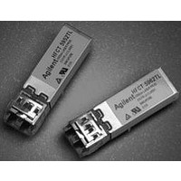
AFCT-5971ALZ Avago Technologies US Inc., AFCT-5971ALZ Datasheet - Page 9
AFCT-5971ALZ
Manufacturer Part Number
AFCT-5971ALZ
Description
TXRX FE SM LASER 125MBS 2X5
Manufacturer
Avago Technologies US Inc.
Datasheet
1.AFCT-5971LZ.pdf
(15 pages)
Specifications of AFCT-5971ALZ
Applications
Ethernet
Data Rate
125MBd
Wavelength
1300nm
Voltage - Supply
3.1 V ~ 3.5 V
Connector Type
LC Duplex
Mounting Type
Through Hole
Data Rate Max
0.125Gbps
Supply Voltage
3.3V
Wavelength Typ
1300nm
Leaded Process Compatible
Yes
Optical Fiber Type
TX/RX
Data Transfer Rate
155Mbps
Optical Rise Time
2/2.2ns
Optical Fall Time
2/2.2ns
Operating Temperature Classification
Industrial
Peak Wavelength
1360/1580nm
Package Type
DIP With Connector
Operating Supply Voltage (min)
3.1V
Operating Supply Voltage (typ)
3.3V
Operating Supply Voltage (max)
3.5V
Output Current
50mA
Operating Temp Range
-40C to 85C
Mounting
Snap Fit To Panel
Pin Count
10
Product
Transceiver
Maximum Rise Time
2 ns, 2.2 ns
Maximum Fall Time
2 ns, 2.2 ns
Maximum Output Current
50 mA
Operating Supply Voltage
3.1 V to 3.5 V
Maximum Operating Temperature
+ 85 C
Minimum Operating Temperature
- 40 C
Package / Case
DIP-10 with Connector
Function
Applications specified for signal rate of 125 MBd, for Fast Ethernet, and Singlemode Fiber.
Lead Free Status / RoHS Status
Lead free / RoHS Compliant
For Use With
Singlemode Glass
Lead Free Status / RoHS Status
Lead free / RoHS Compliant, Lead free / RoHS Compliant
Available stocks
Company
Part Number
Manufacturer
Quantity
Price
Company:

Part Number:
AFCT-5971ALZ
Manufacturer:
Avago Technologies
Quantity:
135


DIMENSIONS IN MILLIMETERS (INCHES)
The AFCT-5971LZ/ALZ is intrinsically eye safe and does
not require shut down circuitry.
Signal Detect
The Signal Detect circuit provides a deasserted output
signal when the optical link is broken (or when the re-
mote transmitter is OFF). The Signal Detect threshold is
set to transition from a high to low state between the
minimum receiver input optical power and -45 dBm
avg. input optical power indicating a definite optical
fault (e.g. unplugged connector for the receiver or
transmitter, broken fiber, or failed far-end transmitter or
data source). The Signal Detect does not detect receiver
data error or error-rate. Data errors can be determined
by signal processing offered by upstream PHY ICs.
Electromagnetic Interference (EMI)
One of a circuit board designer’s foremost concerns is
the control of electromagnetic emissions from electron-
ic equipment. Success in controlling generated Electro-
Figure 7. Recommended Board Layout Hole Pattern
9
(0.525)
(0.299)
13.34
7.59
2 x Ø 2.29 MAX.
(0.118)
3
(0.09)
(0.055 ±0.004)
2 x Ø 1.4 ±0.1
*4
(0.236)
(0.118)
6
3
(0.28)
7.11
(0.18)
4.57
(0.700)
(0.055 ±0.004)
2 x Ø 1.4 ±0.1
17.8
4 x 1.78
(0.07)
(0.121)
3.08
(0.079)
(0.14)
3.56
2
10.16
(0.4)
(0.378)
magnetic Interference (EMI) enables the designer to pass
a governmental agency’s EMI regulatory standard and
more importantly, it reduces the possibility of interfer-
ence to neighboring equipment. Avago Technologies
has designed the AFCT-5971LZ/ALZ to provide excel-
lent EMI performance. The EMI performance of a chassis
is dependent on physical design and features which
help improve EMI suppression. Avago Technologies en-
courages using standard RF suppression practices and
avoiding poorly EMI-sealed enclosures.
Avago Technologies’ LC transceivers (AFCT-5971LZ/ALZ)
have nose shields which provide a convenient chassis
connection to the nose of the transceiver. This nose
shield improves system EMI performance by effec-
tively closing off the LC aperture. The recommended
transceiver position, PCB layout and panel opening for
these devices are the same, making them mechanically
drop-in compatible. Figure 8 shows the recommended
positioning of the transceivers with respect to the PCB
and faceplate.
9.59
10 x Ø 0.81 ±0.1
(0.032 ±0.004)
2 x Ø 2.29
(0.09)
(0.055 ±0.004)
4 x Ø 1.4 ±0.1
*5
(0.079)
2
NOTES:
1. THIS
2. THE HATCHED AREAS ARE KEEP-OUT AREAS
3. 2 x 5 TRANSCEIVER MODULE REQUIRES 16
*4. THE MOUNTING STUDS SHOULD BE
*5. HOLES FOR OPTIONAL HOUSING LEADS
RECOMMENDED CIRCUIT BOARD LAYOUT
FOR THE SFF TRANSCEIVER.
RESERVED FOR HOUSING STANDOFFS. NO
METAL TRACES OR GROUND CONNECTION
IN KEEP-OUT AREAS.
PCB HOLES (10 I/O PINS, 2 SOLDER POSTS
AND 4 OPTIONAL PACKAGE GROUNDING
TABS). PACKAGE GROUNDING TABS
SHOULD BE CONNECTED TO SIGNAL
GROUND.
SOLDERED TO CHASSIS GROUND FOR
MECHANICAL INTEGRITY AND TO ENSURE
FOOTPRINT COMPATIBILITY WITH OTHER
SFF TRANSCEIVERS.
MUST BE TIED TO SIGNAL GROUND.
FIGURE
DESCRIBES
MSA
Related parts for AFCT-5971ALZ
Image
Part Number
Description
Manufacturer
Datasheet
Request
R

Part Number:
Description:
TXRX OPT 1X9 155MB/S 1300NM BK
Manufacturer:
Avago Technologies US Inc.
Datasheet:

Part Number:
Description:
TXRX OPT SFF PLUGGABLE BAIL
Manufacturer:
Avago Technologies US Inc.
Datasheet:
Part Number:
Description:
TXRX OPT SFF PLUGGABLE BAIL DMI
Manufacturer:
Avago Technologies US Inc.
Datasheet:

Part Number:
Description:
TXRX 125MBD DUPLEX BLACK SC 1X9
Manufacturer:
Avago Technologies US Inc.
Datasheet:
Part Number:
Description:
TXRX 125MBD DUPLEX BLUE SC 1X9
Manufacturer:
Avago Technologies US Inc.
Datasheet:

Part Number:
Description:
TXRX OPT SM 155MBS SONET OC3/SDH
Manufacturer:
Avago Technologies US Inc.
Datasheet:
Part Number:
Description:
TXRX SFF SM OC3/STM-1 BAIL DMI
Manufacturer:
Avago Technologies US Inc.
Datasheet:
Part Number:
Description:
TXRX 125MBD DUPLEX BLACK SC 1X9
Manufacturer:
Avago Technologies US Inc.
Datasheet:
Part Number:
Description:
TXRX 125MBD DUPLEX BLUE SC 1X9
Manufacturer:
Avago Technologies US Inc.
Datasheet:

Part Number:
Description:
TXRX OPT SM 155MBS SONET OC3/SDH
Manufacturer:
Avago Technologies US Inc.
Datasheet:

Part Number:
Description:
OPTOCOUPLER GATE DRV 2A 16-SOIC
Manufacturer:
Avago Technologies US Inc.
Datasheet:
Part Number:
Description:
OPTOCOUPLER 2CH 2.5A 16-SOIC
Manufacturer:
Avago Technologies US Inc.
Datasheet:

Part Number:
Description:
OPTOCOUPLER GATE DRV 0.4A 16SOIC
Manufacturer:
Avago Technologies US Inc.
Datasheet:

Part Number:
Description:
OPTOCOUPLER 2.0A 250KHZ 8-DIP
Manufacturer:
Avago Technologies US Inc.
Datasheet:

Part Number:
Description:
OPTOCOUPLER 2.0A 250KHZ GW 8-SMD
Manufacturer:
Avago Technologies US Inc.
Datasheet: