STEVAL-SCM001V1 STMicroelectronics, STEVAL-SCM001V1 Datasheet - Page 14
STEVAL-SCM001V1
Manufacturer Part Number
STEVAL-SCM001V1
Description
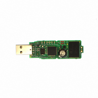
KIT DEMO DONGLE RTC M41T62/ST7
Manufacturer
STMicroelectronics
Datasheets
1.M41T62Q6F.pdf
(43 pages)
2.STEVAL-SCM001V1.pdf
(4 pages)
3.STEVAL-SCM001V1.pdf
(4 pages)
Specifications of STEVAL-SCM001V1
Design Resources
STEVAL-SCM001V1 Gerber Files STEVAL-SCM001V1/RTC Schematic
Main Purpose
Timing, ARM7 based RTC USB Dongle
Embedded
Yes, MCU, 8-Bit
Utilized Ic / Part
M41T62, ST72F651
Primary Attributes
RTC (Real-Time Clock) and Mass Storage Capabilities
Secondary Attributes
Graphical User Interface, USB Interface
Silicon Manufacturer
ST Micro
Silicon Core Number
M41T62 And ST72651AR6
Kit Application Type
Clock & Timing
Application Sub Type
RTC Dongle
Kit Contents
Board CD Docs
Lead Free Status / RoHS Status
Lead free / RoHS Compliant
Other names
497-5684
Available stocks
Company
Part Number
Manufacturer
Quantity
Price
Company:

Part Number:
STEVAL-SCM001V1
Manufacturer:
STMicroelectronics
Quantity:
135


Operation
2.2
Note:
14/43
Figure 15. Acknowledgement sequence
READ mode
In this mode the master reads the M41T6x slave after setting the slave address (see
Figure 17 on page
acknowledge bit, the word address 'An' is written to the on-chip address pointer. Next the
START condition and slave address are repeated followed by the READ mode control bit
(R/W=1). At this point the master transmitter becomes the master receiver. The data byte
which was addressed will be transmitted and the master receiver will send an acknowledge
bit to the slave transmitter. the address pointer is only incremented on reception of an
acknowledge clock. The M41T6x slave transmitter will now place the data byte at address
An+1 on the bus, the master receiver reads and acknowledges the new byte and the
address pointer is incremented to “An+2.”
This cycle of reading consecutive addresses will continue until the master receiver sends a
STOP condition to the slave transmitter.
The system-to-user transfer of clock data will be halted whenever the address being read is
a clock address (00h to 07h). The update will resume due to a stop condition or when the
pointer increments to any non-clock address (08h-0Fh).
This is true both in READ mode and WRITE mode.
An alternate READ mode may also be implemented whereby the master reads the M41T6x
slave without first writing to the (volatile) address pointer. The first address that is read is the
last one stored in the pointer (see
Figure 16. Slave address location
SCL FROM
MASTER
DATA OUTPUT
BY TRANSMITTER
DATA OUTPUT
BY RECEIVER
15). Following the WRITE mode control bit (R/W=0) and the
START
START
MSB
Doc ID 10397 Rev 15
1
Figure 18 on page
1
1
SLAVE ADDRESS
0
1
2
0
0
15).
0
R/W
A
LSB
8
ACKNOWLEDGEMENT
CLOCK PULSE FOR
M41T62/63/64/65
9
AI00601
AI00602
Related parts for STEVAL-SCM001V1
Image
Part Number
Description
Manufacturer
Datasheet
Request
R

Part Number:
Description:
DEMO BOARD FOR SINGLE OP-AMPS
Manufacturer:
STMicroelectronics
Datasheet:

Part Number:
Description:
KIT EVAL USB/RS232 ST7
Manufacturer:
STMicroelectronics
Datasheet:

Part Number:
Description:
BOARD EVAL HDMI $ VIDEO SWITCH
Manufacturer:
STMicroelectronics
Datasheet:

Part Number:
Description:
BOARD DEMO MEMS LPR430AL
Manufacturer:
STMicroelectronics
Datasheet:

Part Number:
Description:
BOARD EVALUATION FOR LPR550AL
Manufacturer:
STMicroelectronics
Datasheet:

Part Number:
Description:
EVAL BOARD A/D TS4657
Manufacturer:
STMicroelectronics
Datasheet:

Part Number:
Description:
BOARD & REF DESIGN
Manufacturer:
STMicroelectronics
Datasheet:

Part Number:
Description:
BOARD EVAL S-TOUCH STM32
Manufacturer:
STMicroelectronics
Datasheet:

Part Number:
Description:
BOARD ADAPTER LPR403AL DIL24
Manufacturer:
STMicroelectronics
Datasheet:

Part Number:
Description:
BOARD DEMO LPR4150AL GYROSCOPE
Manufacturer:
STMicroelectronics
Datasheet:
Part Number:
Description:
STMicroelectronics [RIPPLE-CARRY BINARY COUNTER/DIVIDERS]
Manufacturer:
STMicroelectronics
Datasheet:
Part Number:
Description:
STMicroelectronics [LIQUID-CRYSTAL DISPLAY DRIVERS]
Manufacturer:
STMicroelectronics
Datasheet:

Part Number:
Description:
BOARD EVAL FOR MEMS SENSORS
Manufacturer:
STMicroelectronics
Datasheet: