DEMO9S08MP16 Freescale Semiconductor, DEMO9S08MP16 Datasheet - Page 26
DEMO9S08MP16
Manufacturer Part Number
DEMO9S08MP16
Description
BOARD DEMO FOR MC9S08MP16
Manufacturer
Freescale Semiconductor
Specifications of DEMO9S08MP16
Main Purpose
Power Management, Motor Control
Embedded
*
Utilized Ic / Part
MC9S08MP16
Primary Attributes
*
Secondary Attributes
*
Processor To Be Evaluated
MC9S08MP16
Interface Type
RS232, USB
Operating Supply Voltage
6 V
Silicon Manufacturer
Freescale
Core Architecture
HCS08
Core Sub-architecture
HCS08
Silicon Core Number
MC9S08
Silicon Family Name
S08MP
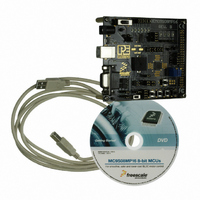
Kit Contents
Demo Board USB Cable DVD
Rohs Compliant
Yes
Tool Type
Demonstration Board
Cpu Core
HCS08
Data Bus Width
8 bit
Lead Free Status / RoHS Status
Lead free / RoHS Compliant


7.4
7.5
7.5.1
22
Figure 7-4: Jumper Settings for Input Signals to P&E’s Embedded Multilink, P&E
External Crystal Circuitry
Input and Reset Switches
J9 - P&E’s Logic Analyzer Inputs IN0/IN1
The DEMO9S08MP16 design has incorporated an external crystal circuitry,
but its components are not populaTED. The user may populate the
components and use the jumpers in header J7 to connect the crystal circuitry
to the processor.
The DEMO9S08MP16 has 4 switches that are connected to signals PTD4,
PTD5, PTD6, and PTD7 respectively, and are enabled or disabled by the 4
corresponding jumpers KEY_ENABLE (J12).
The DEMO9S08MP16 has an option to connect two signals, PTA2 and PTA3,
to the Embedded Multilink for signal processing. The two signals are
connected or disconnected to IN0 or IN1 correspondingly via jumper P&E
INPUT_EN (J9).
The DEMO9S08MP16 has one Reset switch and one Reset LED associated
with it. These are enabled or disabled by the two corresponding jumper
RESET_EN (J23).
The logic analyzer inputs are marked on one side of the J9 jumper. The inputs
allow P&E’s PC-based logic analyzer application to display these signals in
real-time.
By installing both jumpers, the logic analyzer pins IN0 and IN1 will be
connected to PTA2 and PTA3 respectively.
By removing these jumpers IN0 and IN1 will be unconnected. The
user may connect these signals, via wires, to any other signals on the
processor which they wish to view on the PC.
DEMO9S08MP16 User Manual
Related parts for DEMO9S08MP16
Image
Part Number
Description
Manufacturer
Datasheet
Request
R

Part Number:
Description:
Manufacturer:
Freescale Semiconductor, Inc
Datasheet:
Part Number:
Description:
Manufacturer:
Freescale Semiconductor, Inc
Datasheet:
Part Number:
Description:
Manufacturer:
Freescale Semiconductor, Inc
Datasheet:
Part Number:
Description:
Manufacturer:
Freescale Semiconductor, Inc
Datasheet:
Part Number:
Description:
Manufacturer:
Freescale Semiconductor, Inc
Datasheet:
Part Number:
Description:
Manufacturer:
Freescale Semiconductor, Inc
Datasheet:
Part Number:
Description:
Manufacturer:
Freescale Semiconductor, Inc
Datasheet:
Part Number:
Description:
Manufacturer:
Freescale Semiconductor, Inc
Datasheet:
Part Number:
Description:
Manufacturer:
Freescale Semiconductor, Inc
Datasheet:
Part Number:
Description:
Manufacturer:
Freescale Semiconductor, Inc
Datasheet:
Part Number:
Description:
Manufacturer:
Freescale Semiconductor, Inc
Datasheet:
Part Number:
Description:
Manufacturer:
Freescale Semiconductor, Inc
Datasheet:
Part Number:
Description:
Manufacturer:
Freescale Semiconductor, Inc
Datasheet:
Part Number:
Description:
Manufacturer:
Freescale Semiconductor, Inc
Datasheet:
Part Number:
Description:
Manufacturer:
Freescale Semiconductor, Inc
Datasheet: