KIT33880DWBEVB Freescale Semiconductor, KIT33880DWBEVB Datasheet - Page 14
KIT33880DWBEVB
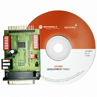
Manufacturer Part Number
KIT33880DWBEVB
Description
KIT EVAL FOR MC33880 8X SW W/SPI
Manufacturer
Freescale Semiconductor
Specifications of KIT33880DWBEVB
Main Purpose
Power Management, High & Low Side Driver (Internal FET)
Embedded
No
Utilized Ic / Part
MC33880
Primary Attributes
8 Configurable High/Low FETs, 5.5 ~ 24.5V, 0.8 ~ 2A, 0.55 Ohm
Secondary Attributes
SPI Interface, Reverse Battery, Temperature, Short Circuit, Current Limit Protection
Lead Free Status / RoHS Status
Contains lead / RoHS non-compliant


LOGIC POWER (VDD)
is used for power-on reset (POR). To achieve low standby
current on V
V
V
OPEN DRAIN OUTPUT (D1 – D8)
For High-Side Drive configurations, the drain pins are
connected to battery supply. In Low-Side Drive
configurations, the drain pins are connected to the low side of
14
33880
FUNCTIONAL DESCRIPTION
DD
DD
The V
The D1 – D8 pins are the open drain outputs of the 33880.
pin. The device will be in reset with all drivers off when
is below 3.9 V
DD
pin supplies logic power to the 33880 device and
PWR
supply, power must be removed from the
DC
.
the load. All outputs may be configured individually as
desired. When Low-Side Drive is used, the 33880 limits the
positive transient for inductive loads to 45 V.
SOURCE OUTPUT (S1 – S8)
High-Side Drive configurations, the source pins are
connected directly to the load. In Low-Side Drive
configurations the source is connected to ground. All outputs
may be configured individually as desired. When High-Side
drive is used, the 33880 will limit the negative transient for
inductive loads to -20 V.
The S1 – S8 pins are the source outputs of the 33880. For
Analog Integrated Circuit Device Data
Freescale Semiconductor
Related parts for KIT33880DWBEVB
Image
Part Number
Description
Manufacturer
Datasheet
Request
R

Part Number:
Description:
Manufacturer:
Freescale Semiconductor, Inc
Datasheet:
Part Number:
Description:
Manufacturer:
Freescale Semiconductor, Inc
Datasheet:
Part Number:
Description:
Manufacturer:
Freescale Semiconductor, Inc
Datasheet:
Part Number:
Description:
Manufacturer:
Freescale Semiconductor, Inc
Datasheet:
Part Number:
Description:
Manufacturer:
Freescale Semiconductor, Inc
Datasheet:
Part Number:
Description:
Manufacturer:
Freescale Semiconductor, Inc
Datasheet:
Part Number:
Description:
Manufacturer:
Freescale Semiconductor, Inc
Datasheet:
Part Number:
Description:
Manufacturer:
Freescale Semiconductor, Inc
Datasheet:
Part Number:
Description:
Manufacturer:
Freescale Semiconductor, Inc
Datasheet:
Part Number:
Description:
Manufacturer:
Freescale Semiconductor, Inc
Datasheet:
Part Number:
Description:
Manufacturer:
Freescale Semiconductor, Inc
Datasheet:
Part Number:
Description:
Manufacturer:
Freescale Semiconductor, Inc
Datasheet:
Part Number:
Description:
Manufacturer:
Freescale Semiconductor, Inc
Datasheet:
Part Number:
Description:
Manufacturer:
Freescale Semiconductor, Inc
Datasheet:
Part Number:
Description:
Manufacturer:
Freescale Semiconductor, Inc
Datasheet: