DK-SI-4S100G2N Altera, DK-SI-4S100G2N Datasheet - Page 22
DK-SI-4S100G2N
Manufacturer Part Number
DK-SI-4S100G2N
Description
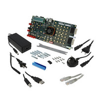
KIT DEV STRATIX IV TRANSCEIVER
Manufacturer
Altera
Series
Stratix® IVr
Datasheet
1.DK-SI-4S100G2N.pdf
(28 pages)
Specifications of DK-SI-4S100G2N
Main Purpose
*
Embedded
*
Utilized Ic / Part
EP4S100G2F40C2ES1
Primary Attributes
*
Secondary Attributes
*
Silicon Manufacturer
Altera
Core Architecture
FPGA
Core Sub-architecture
Stratix
Silicon Core Number
EP4S
Silicon Family Name
Stratix IV GT
Rohs Compliant
Yes
Lead Free Status / RoHS Status
Lead free / RoHS Compliant
Other names
544-2603


A–2
Custom User Design
Creating Flash Files Using the Nios II EDS
sof2flash --input=yourfile_hw.sof --output=yourfile_hw.flash --offset=0xC20000 r
Transceiver Signal Integrity Development Kit, Stratix IV GT Edition User Guide
1
c
Table A–1. Byte Address Flash Memory Map (Part 2 of 2)
Using the Board Update Portal or Nios II EDS tools, you can update the user flash
configuration with designs provided on Altera’s website for demonstration and
evaluation. For more information, refer to
Altera advises against overwriting the FACTORY HW or SW images unless you are
expert with the Altera tools or overwriting the factory design is deliberate. If you
unintentionally overwrite the FACTORY HW or SW images, refer to
Factory Design to the Flash Device” on page
As you develop your own project using the Altera tools, you may wish to program the
flash device so that, upon power up, it loads the FPGA with your own user design.
With the Nios II EDS tool sof2flash, your Quartus II compiled .sof can be converted to
a .flash file. The .flash file can then be written to the user hardware location of the
flash memory using either the Board Update Portal or the Nios II EDS
nios2-flash-programmer from a Nios II command-line shell.
If you used the Nios II EDS to derive your software design, you can use the Nios II
EDS tools to convert your compiled and linked software Executable and Linkable
Format File (.elf) design to .flash files. After your design files are in the .flash format,
then both hardware and software files can be written using the Board Update Portal
or using the Nios II EDS nios2-flash-programmer.
For more information about Nios II EDS software tools and practices, refer to
www.altera.com/products/ip/processors/nios2/tools/ni2-development_tools.html
The following sections describe how to program the flash device using first the Board
Update Portal, then using only the Nios II EDS command-line tools.
If you have hardware developed using the Quartus II application, and software
developed using the Nios II EDS, follow these instructions:
1. On the Windows Start Menu, go to All Programs> altera> Nios II EDS> Nios II
2. In the Nios II Command Shell, navigate to the directory where your design files
Reserved
Ethernet option bits
User design reset vector
Command Shell.
are located and type the following Nios II EDS commands:
■
■
For .sof Quartus II hardware files:
For .elf Nios II software files:
Block Description
Size
32 KB
32 KB
32 KB
“Board Update Portal” on page
A–4.
0x00010000 - 0x00017FFF
0x00008000 - 0x0000FFFF
0x00000000 - 0x00007FFF
Appendix A: Programming the Flash Device
Address Range
Creating Flash Files Using the Nios II EDS
© December 2009 Altera Corporation
“Restoring the
5–1.
Related parts for DK-SI-4S100G2N
Image
Part Number
Description
Manufacturer
Datasheet
Request
R

Part Number:
Description:
KIT DEV STRATIX IV 4SGX230N/C2
Manufacturer:
Altera
Datasheet:

Part Number:
Description:
SI KIT W/SII GX EP2SGX90N
Manufacturer:
Altera
Datasheet:

Part Number:
Description:
KIT DEV STRATIX V FPGA 5SGXEA7
Manufacturer:
Altera
Datasheet:

Part Number:
Description:
Programmable Logic IC Development Tools FPGA Starter Kit For Stratix V 5SGXEA7
Manufacturer:
Altera Corporation
Part Number:
Description:
Programmable Logic IC Development Tools FPGA Starter Kit For Stratix V 5SGTMC7
Manufacturer:
Altera Corporation
Part Number:
Description:
Programmable Logic IC Development Tools FPGA Starter Kit For Stratix V 5SGTMC7 ES
Manufacturer:
Altera Corporation

Part Number:
Description:
CYCLONE II STARTER KIT EP2C20N
Manufacturer:
Altera
Datasheet:
Part Number:
Description:
CPLD, EP610 Family, ECMOS Process, 300 Gates, 16 Macro Cells, 16 Reg., 16 User I/Os, 5V Supply, 35 Speed Grade, 24DIP
Manufacturer:
Altera Corporation
Datasheet:
Part Number:
Description:
CPLD, EP610 Family, ECMOS Process, 300 Gates, 16 Macro Cells, 16 Reg., 16 User I/Os, 5V Supply, 15 Speed Grade, 24DIP
Manufacturer:
Altera Corporation
Datasheet:
Part Number:
Description:
Manufacturer:
Altera Corporation
Datasheet:
Part Number:
Description:
CPLD, EP610 Family, ECMOS Process, 300 Gates, 16 Macro Cells, 16 Reg., 16 User I/Os, 5V Supply, 30 Speed Grade, 24DIP
Manufacturer:
Altera Corporation
Datasheet:
Part Number:
Description:
High-performance, low-power erasable programmable logic devices with 8 macrocells, 10ns
Manufacturer:
Altera Corporation
Datasheet:
Part Number:
Description:
High-performance, low-power erasable programmable logic devices with 8 macrocells, 7ns
Manufacturer:
Altera Corporation
Datasheet: