VSUPEV2 Microchip Technology, VSUPEV2 Datasheet - Page 17
VSUPEV2
Manufacturer Part Number
VSUPEV2
Description
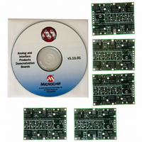
BOARD EVAL FOR MCP4022,4023,4024
Manufacturer
Microchip Technology
Specifications of VSUPEV2
Main Purpose
Power Management, Power Supply Supervisor/Tracker/Sequencer
Embedded
No
Utilized Ic / Part
SOT-23-5, SOT-23-6 Package
Primary Attributes
Voltage Detector & Supervisor
Secondary Attributes
5 Boards & 3 IC's Included
Processor To Be Evaluated
SOT23-5/6
Lead Free Status / RoHS Status
Lead free / RoHS Compliant
Lead Free Status / RoHS Status
Lead free / RoHS Compliant, Lead free / RoHS Compliant


Installation and Operation
2.3.1
The Hardware
Figure 2-2 shows the layout of the Voltage Supervisor SOT-23-5/6 Evaluation Board.
This is a small four-layer board (1.5" x 2" (38.1 mm x 50.8 mm)). There are six
connection points/pads that can use either through-hole or surface-mount connector
posts.
Additionally, a test point is available between the device pin and the PCB pad that may
be useful if the in-line resistor (R1A, R1C, R1D or R1E) is installed.
The different SOT-23 layout options are outlined in Section 2.4.3 “SOT-23-6 and
SOT-23-5 Footprints”, with Opt A, Opt B, Opt C, Opt D and Opt E indicating the layout
option of that SOT-23-5/6 footprint.
There are six pads on the PCB. One is labeled VDD, one is labeled VSS, with all pads
having a label that indicates the footprint option used (shown as “A B C D E”) and a
label underneath that indicates the pin number of that footprint. This footprint option/pin
number combination will be used to indicate the remaining pads. If the device is placed
in the option A footprint, the remaining pads would be A1, A3, A4 and A6, where the
VDD pad is also A6 and the VSS pad is A2. Figure 2-2 has text added on each pad to
show what the “pad name” would be (A1, A2, A3, A4, A5 and A6). If the device required
the option C footprint, what is currently A1 for option A would then be referred to as pad
C6 for option C.
Each of these four pads has four passive components associated with them. A pull-up
resistor, a pull-down resistor, an in-line resistor and a filtering/load capacitor. The
pull-up resistor is always R2x, the pull-down resistor is R3x, the in-line resistor is R1x
and the filtering/load capacitor is C5x. The “x” is an alpha character that corresponds
to a particular pad. So pad A1’s pull-up resistor is R2A.
The green area of Figure 2-2 shows the silk screen on the bottom layer of the PCB.
This is where the details of the implemented circuit can be written.
Resistor R2x is a pull-up resistor that may need to be installed for devices with an
open-drain output. Though resistor R3x is not currently required, it was placed for
possible future requirements. Resistor R1x is not required, but may be useful if this
board is to be interfaced into existing circuits. If resistor R1x is to be installed, remem-
ber to cut the trace that “shorts out” R3. Capacitors C1, C2, C3, C4, C6, C5A, C5C,
C5D, C5E and C5F are bypass capacitors that may be required to be installed, depend-
ing on the device selected and the system requirements (such as the noise present on
the power supply). Table 2-3 describes the components.
© 2006 Microchip Technology Inc.
DS51527B-page 13
Related parts for VSUPEV2
Image
Part Number
Description
Manufacturer
Datasheet
Request
R

Part Number:
Description:
Manufacturer:
Microchip Technology Inc.
Datasheet:
Part Number:
Description:
Manufacturer:
Microchip Technology Inc.
Datasheet:
Part Number:
Description:
Manufacturer:
Microchip Technology Inc.
Datasheet:
Part Number:
Description:
Manufacturer:
Microchip Technology Inc.
Datasheet:
Part Number:
Description:
Manufacturer:
Microchip Technology Inc.
Datasheet:
Part Number:
Description:
Manufacturer:
Microchip Technology Inc.
Datasheet:
Part Number:
Description:
Manufacturer:
Microchip Technology Inc.
Datasheet:
Part Number:
Description:
Manufacturer:
Microchip Technology Inc.
Datasheet: