MXSIGDM Microchip Technology, MXSIGDM Datasheet - Page 16
MXSIGDM
Manufacturer Part Number
MXSIGDM
Description
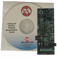
BOARD DEMO PICTAIL MIXED SIGNAL
Manufacturer
Microchip Technology
Series
PICtail™r
Datasheet
1.MXSIGDM.pdf
(54 pages)
Specifications of MXSIGDM
Main Purpose
Mixed Signal for MCU: ADC, DAC,
Embedded
Yes, MCU, 8-Bit
Utilized Ic / Part
TX132x,MCP330x,320x,494x,3221,3201,1525,1541
Primary Attributes
3 ADCs, 3 DACs, 2 Voltage References, 5V LDO
Secondary Attributes
DIP Switches, 2 LEDs, PIC16F767
Processor To Be Evaluated
TC132x, MCP330x, MCP320x, MCP492x, MCP3221, MCP3021, MCP15x
Interface Type
I2C, SPI
Lead Free Status / RoHS Status
Contains lead / RoHS non-compliant
Lead Free Status / RoHS Status
Lead free / RoHS Compliant, Contains lead / RoHS non-compliant


DS51523A-page 12
TABLE 2-1:
V
V
CS0
SCK/SCL
SDI/SDA
SDO
CS1
LDAC
V
LED0/TX
LED1/RX
SW0
SW1
SW2
Legend: TTL = TTL compatible input
Pin Name
SS
IN
REF_ADC
I = Input
Number
Pin
14
13
12
11
10
9
8
7
6
5
4
3
2
1
PICkit™ 1 FLASH STARTER KIT 14-PIN HEADER INTERFACE
PINS
Type
Pin
I/O
I/O
—
—
O
O
O
O
O
O
I
I
I
I
Buffer
Type
ST
ST
—
—
—
—
—
—
—
—
—
—
—
—
Electrical Ground. Both analog and digital.
Power Supply Input. Refer to Note 2 in Appendix A
“Schematics and Layouts”. Do not plug in 9V
supply and connect to PICkit™ 1 Flash Starter Kit.
SPI™ Chip Select signal for the external ADCs. Do
not populate both the MCP3551 and the MCP3302
as they share the same CS0 signal.
SPI Clock or I
weak pull-up R
SPI Data In or I
Note that external weak pull-up R
nal to V
SPI Data Out Signal (Data In on DAC and ADC)
SPI Chip Select Signal for the External DACs. Do not
populate both the MCP492X and the MCP482X as
they share the same CS0 signal.
Latches the DAC Output When Low. Note the weak
pull-down resistor R
pin to a desired state.
JP4 selects the V
reference signal. The PICmicro
the PICkit™ 1 Flash Starter Kit may use this for its
internal ADC’s V
Active High Red LED Signal. This I/O also has the
USART’s TX signal multiplexed on it.
Active High Green LED Signal. This I/O also has the
USART’s RX signal multiplexed on it.
S1’s Switch 1. This pin uses the internal pull-up resis-
tor to determine when the switch is open.
S1’s Switch 2. This pin uses the internal pull-up resis-
tor to determine when the switch is open.
S1’s Switch 3. This pin uses the internal pull-up resis-
tor to determine when the switch is open.
ST = Schmitt Trigger input with CMOS levels
O = Output
DD2
.
2
C™ Clock Signal. Note that external
20
2
C Data signal (Data Out on ADC).
REF
REF
connects this signal to V
5
.
Description
if the firmware doesn’t drive the
source to use as the ADC
2004 Microchip Technology Inc.
®
microcontroller on
14
connects this sig-
DD2
.
Related parts for MXSIGDM
Image
Part Number
Description
Manufacturer
Datasheet
Request
R

Part Number:
Description:
Manufacturer:
Microchip Technology Inc.
Datasheet:
Part Number:
Description:
Manufacturer:
Microchip Technology Inc.
Datasheet:
Part Number:
Description:
Manufacturer:
Microchip Technology Inc.
Datasheet:
Part Number:
Description:
Manufacturer:
Microchip Technology Inc.
Datasheet:
Part Number:
Description:
Manufacturer:
Microchip Technology Inc.
Datasheet:
Part Number:
Description:
Manufacturer:
Microchip Technology Inc.
Datasheet:
Part Number:
Description:
Manufacturer:
Microchip Technology Inc.
Datasheet:
Part Number:
Description:
Manufacturer:
Microchip Technology Inc.
Datasheet: