MCP3421DM-BFG Microchip Technology, MCP3421DM-BFG Datasheet - Page 18
MCP3421DM-BFG
Manufacturer Part Number
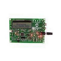
MCP3421DM-BFG
Description
BOARD DEMO FOR MCP3421
Manufacturer
Microchip Technology
Datasheets
1.MCP3421A2T-ECH.pdf
(42 pages)
2.MCP3421DM-BFG.pdf
(26 pages)
3.MCP3421A0T-ECH.pdf
(30 pages)
Specifications of MCP3421DM-BFG
Main Purpose
Power Management, Battery Gauge
Utilized Ic / Part
MCP3421
Processor To Be Evaluated
MCP3421
Lead Free Status / RoHS Status
Lead free / RoHS Compliant
Secondary Attributes
-
Embedded
-
Primary Attributes
-
Lead Free Status / RoHS Status
Lead free / RoHS Compliant, Lead free / RoHS Compliant


MCP3421
TABLE 5-4:
DS22003D-page 18
Electrical Specifications: Unless otherwise specified, all limits are specified for T
V
Standard Mode
Clock frequency
Clock high time
Clock low time
SDA and SCL rise time
SDA and SCL fall time
START condition hold time
Repeated START condition
setup time
Data hold time
Data input setup time
STOP condition setup time
STOP condition hold time
Output valid from clock
(Notes 2 and 3)
Bus free time
Fast Mode
Clock frequency
Clock high time
Clock low time
SDA and SCL rise time
SDA and SCL fall time
START condition hold time
Repeated START condition
setup time
Data hold time
Data input setup time
STOP condition setup time
STOP condition hold time
Output valid from clock
(Notes 2 and 3)
Bus free time
Input filter spike suppression
(Note 5)
Note 1:
SS
= 0V, V
2:
3:
4:
5:
Parameters
This parameter is ensured by characterization and not 100% tested.
This specification is not a part of the I
plus SDA Fall (or rise) time:
If this parameter is too short, it can create an unintended Start or Stop condition to other devices on the bus line. If this
parameter is too long, Clock Low time (T
For Data Input: This parameter must be longer than t
Clock Low time (T
For Data Output: This parameter is characterized, and tested indirectly by testing T
This parameter is ensured by characterization and not 100% tested. This parameter is not available for Standard Mode.
IN
+ = V
(Note 3)
(Note 4)
I
2
IN
C SERIAL TIMING SPECIFICATIONS
- = V
(Note 1)
(Note 1)
(Note 1)
(Note 1)
REF
LOW
/2.
) can be affected.
T HD:DAT
T SU:STO
T HD:STD
T HD:DAT
T SU:STO
T HD:STD
T HD:STA
T SU:STA
T SU:DAT
T HD:STA
T SU:STA
T SU:DAT
T HIGH
T HIGH
T LOW
T LOW
Sym
T BUF
T SCL
T BUF
f
T AA
T AA
T SP
SCL
T R
T F
T R
T F
T AA
= T
20 + 0.1Cb
20 + 0.1Cb
HD:DAT
2
4000
4700
4000
4700
4000
4000
4700
1300
1300
C specification. This specification is equivalent to the Data Hold Time (
250
600
600
600
100
600
600
Min
—
—
0
0
0
0
0
0
0
LOW
+ T
) can be affected.
F
(
OR
T
Typ
—
—
—
—
—
—
—
—
—
—
—
—
—
—
—
—
—
—
—
—
—
—
—
—
—
—
—
SP
R
).
. If this parameter is too long, the Data Input Setup (T
1000
3450
3750
1200
Max
100
300
400
300
300
900
—
—
—
—
—
—
—
—
—
—
—
—
—
—
—
—
50
A
= -40 to +85°C, V
Units
kHz
kHz
ns
ns
ns
ns
ns
ns
ns
ns
ns
ns
ns
ns
ns
ns
ns
ns
ns
ns
ns
ns
ns
ns
ns
ns
ns
AA
© 2007 Microchip Technology Inc.
parameter.
From V
From V
After this period, the first clock
pulse is generated.
Only relevant for repeated Start
condition
Time between START and STOP
conditions.
From V
From V
After this period, the first clock
pulse is generated
Only relevant for repeated Start
condition
Time between START and STOP
conditions.
SDA and SCL pins
DD
= +2.7V, +3.3V or +5.0V,
IL
IH
IL
IH
to V
to V
to V
to V
IH
IH
IL
IL
Conditions
SU:DAT
T HD:DAT
) or
)
Related parts for MCP3421DM-BFG
Image
Part Number
Description
Manufacturer
Datasheet
Request
R

Part Number:
Description:
18-Bit Analog-to-Digital Converter with I2C Interface and On-Board Reference
Manufacturer:
Microchip Technology
Datasheet:

Part Number:
Description:
Manufacturer:
Microchip Technology Inc.
Datasheet:
Part Number:
Description:
Manufacturer:
Microchip Technology Inc.
Datasheet:
Part Number:
Description:
Manufacturer:
Microchip Technology Inc.
Datasheet:
Part Number:
Description:
Manufacturer:
Microchip Technology Inc.
Datasheet:
Part Number:
Description:
Manufacturer:
Microchip Technology Inc.
Datasheet:
Part Number:
Description:
Manufacturer:
Microchip Technology Inc.
Datasheet:
Part Number:
Description:
Manufacturer:
Microchip Technology Inc.
Datasheet:
Part Number:
Description:
Manufacturer:
Microchip Technology Inc.
Datasheet: