MCP3421DM-BFG Microchip Technology, MCP3421DM-BFG Datasheet - Page 6
MCP3421DM-BFG
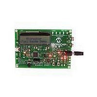
Manufacturer Part Number
MCP3421DM-BFG
Description
BOARD DEMO FOR MCP3421
Manufacturer
Microchip Technology
Datasheets
1.MCP3421A2T-ECH.pdf
(42 pages)
2.MCP3421DM-BFG.pdf
(26 pages)
3.MCP3421A0T-ECH.pdf
(30 pages)
Specifications of MCP3421DM-BFG
Main Purpose
Power Management, Battery Gauge
Utilized Ic / Part
MCP3421
Processor To Be Evaluated
MCP3421
Lead Free Status / RoHS Status
Lead free / RoHS Compliant
Secondary Attributes
-
Embedded
-
Primary Attributes
-
Lead Free Status / RoHS Status
Lead free / RoHS Compliant, Lead free / RoHS Compliant


MCP3421
3.0
The descriptions of the pins are listed in
TABLE 3-1:
3.1
V
MCP3421 device accepts a fully differential analog
input signal which is connected on the V
input pins. The differential voltage that is converted is
defined by V
applied at the V
at the V
programmable gain amplifier (PGA) before the
conversion. The differential input voltage should not
exceed an absolute of (V
measurement, where V
voltage (2.048V) and PGA is the PGA gain setting. The
converter output code will saturate if the input range
exceeds (V
The absolute voltage range on each of the differential
input pins is from V
above or below this range will cause leakage currents
through the Electrostatic Discharge (ESD) diodes at
the input pins. This ESD current can cause unexpected
performance of the device. The common mode of the
analog inputs should be chosen such that both the
differential analog input range and the absolute voltage
range on each pin are within the specified operating
range
Characteristics” and Section 4.0 “Description of
Device Operation”.
3.2
V
requires an appropriate bypass capacitor of about
0.1 µF (ceramic) to ground. An additional 10 µF
capacitor (tantalum) in parallel is also recommended
to further attenuate high frequency noise present in
some application boards. The supply voltage (V
must be maintained in the 2.7V to 5.5V range for spec-
ified operation.
V
device. The user must connect the V
plane through a low impedance connection. If an
analog ground path is available in the application PCB
DS22003D-page 6
IN
DD
SS
+ and V
Pin No
is the ground pin and the current return path of the
is the power supply pin for the device. This pin
1
2
3
4
5
6
IN
PIN DESCRIPTIONS
- pin. The input signal level is amplified by the
Analog Inputs (V
Supply Voltage (V
defined
REF
IN
IN
- are differential signal input pins. The
= (V
/PGA).
IN
+ pin and V
PIN FUNCTION TABLE
IN
SS
Sym
+ - V
V
SCL
SDA
V
V
V
in
-0.3V to V
IN
DD
IN
SS
+
-
REF
IN
-) where V
Section 1.0
is the internal reference
IN
REF
- is the voltage applied
IN
Non-Inverting Analog Input Pin
Ground Pin
Serial Clock Input Pin of the I
Bidirectional Serial Data Pin of the I
Positive Supply Voltage Pin
Inverting Analog Input Pin
DD
DD
/PGA) for accurate
+, V
+0.3V. Any voltage
, V
SS
IN
IN
+ is the voltage
pin to a ground
SS
Table
-)
IN
)
“Electrical
+ and V
3-1.
DD
IN
-
)
2
C Interface
(printed circuit board), it is highly recommended that
the V
isolated within an analog ground plane of the circuit
board.
3.3
SCL is the serial clock pin of the I
MCP3421 acts only as a slave and the SCL pin
accepts only external serial clocks. The input data
from the Master device is shifted into the SDA pin on
the rising edges of the SCL clock and output from the
MCP3421 occurs at the falling edges of the SCL clock.
The SCL pin is an open-drain N-channel driver.
Therefore, it needs a pull-up resistor from the V
to the SCL pin. Refer to Section 5.3 “I
munications” for more details of I
communication.
3.4
SDA is the serial data pin of the I
pin is used for input and output data. In read mode, the
conversion result is read from the SDA pin (output). In
write mode, the device configuration bits are written
(input) though the SDA pin. The SDA pin is an open-
drain N-channel driver. Therefore, it needs a pull-up
resistor from the V
start and stop conditions, the data on the SDA pin must
be stable during the high period of the clock. The high
or low state of the SDA pin can only change when the
clock signal on the SCL pin is low. Refer to Section 5.3
“I
Serial Interface communication.
2
C Serial Communications” for more details of I
2
C Interface
SS
Function
pin be tied to the analog ground path or
Serial Clock Pin (SCL)
Serial Data Pin (SDA)
DD
line to the SDA pin. Except for
© 2007 Microchip Technology Inc.
2
C interface. The SDA
2
2
C Serial Interface
C interface. The
2
C Serial Com-
DD
line
2
C
Related parts for MCP3421DM-BFG
Image
Part Number
Description
Manufacturer
Datasheet
Request
R

Part Number:
Description:
18-Bit Analog-to-Digital Converter with I2C Interface and On-Board Reference
Manufacturer:
Microchip Technology
Datasheet:

Part Number:
Description:
Manufacturer:
Microchip Technology Inc.
Datasheet:
Part Number:
Description:
Manufacturer:
Microchip Technology Inc.
Datasheet:
Part Number:
Description:
Manufacturer:
Microchip Technology Inc.
Datasheet:
Part Number:
Description:
Manufacturer:
Microchip Technology Inc.
Datasheet:
Part Number:
Description:
Manufacturer:
Microchip Technology Inc.
Datasheet:
Part Number:
Description:
Manufacturer:
Microchip Technology Inc.
Datasheet:
Part Number:
Description:
Manufacturer:
Microchip Technology Inc.
Datasheet:
Part Number:
Description:
Manufacturer:
Microchip Technology Inc.
Datasheet: