MCP3421DM-BFG Microchip Technology, MCP3421DM-BFG Datasheet - Page 21
MCP3421DM-BFG
Manufacturer Part Number
MCP3421DM-BFG
Description
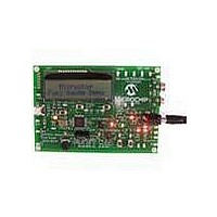
BOARD DEMO FOR MCP3421
Manufacturer
Microchip Technology
Datasheets
1.MCP3421A2T-ECH.pdf
(42 pages)
2.MCP3421DM-BFG.pdf
(26 pages)
3.MCP3421A0T-ECH.pdf
(30 pages)
Specifications of MCP3421DM-BFG
Main Purpose
Power Management, Battery Gauge
Utilized Ic / Part
MCP3421
Processor To Be Evaluated
MCP3421
Lead Free Status / RoHS Status
Lead free / RoHS Compliant
Secondary Attributes
-
Embedded
-
Primary Attributes
-
Lead Free Status / RoHS Status
Lead free / RoHS Compliant, Lead free / RoHS Compliant


6.0
The MCP3421 device can be used for various precision
analog-to-digital converter applications. The device
operates with very simple connections to the
application circuit. The following sections discuss the
examples of the device connections and applications.
6.1
6.1.1
The fully differential input signals can be connected to
the V
within absolute common mode input voltage range:
V
protection diode at the input pin begins to conduct and
the error due to input leakage current increases rapidly.
Within this limit, the differential input V
is boosted by the PGA before a conversion takes place.
The MCP3421 can not accept negative input voltages
on the input pins.
typical connection examples for differential inputs and a
single-ended input, respectively. For the single-ended
input, the input signal is applied to one of the input pins
(typically connected to the V
input pin (typically V
signal range of the single-ended configuration is from
0V to 2.048V. All device characteristics hold for the
single-ended configuration, but this configuration loses
one bit resolution because the input can only stand in
positive half scale. Refer to Section 1.0 “Electrical
Characteristics”.
6.1.2
For accurate measurement, the application circuit
needs a clean supply voltage and must block any noise
signal to the MCP3421 device.
example of using two bypass capacitors (a 10 µF
tantalum capacitor and a 0.1 µF ceramic capacitor) in
parallel on the V
filter out any high frequency noises on the V
also provide the momentary bursts of extra currents
when the device needs from the supply. These
capacitors should be placed as close to the V
possible (within one inch). If the application circuit has
separate digital and analog power supplies, the V
and V
plane.
6.1.3
The SCL and SDA pins of the MCP3421 are open-drain
configurations. These pins require a pull-up resistor as
shown in
resistors depends on the operating speed (standard,
fast, and high speed) and loading capacitance of the
© 2007 Microchip Technology Inc.
SS
- 0.3V to V
IN
SS
+ and V
BASIC APPLICATION
CONFIGURATION
Connecting to the Application
Circuits
of the MCP3421 should reside on the analog
Figure
INPUT VOLTAGE RANGE
BYPASS CAPACITORS ON V
CONNECTING TO I
PULL-UP RESISTORS
IN
DD
DD
- input pins. The input range should be
6-1. The value of these pull-up
line. These capacitors are helpful to
+ 0.3V. Outside this limit, the ESD
Figure 6-1
IN
- pin) is grounded. The input
IN
+ pin) while the other
and
Figure 6-1
2
C BUS USING
Figure 6-2
IN
(= V
DD
IN
shows an
DD
DD
+ - V
line and
pin as
show
PIN
IN
DD
-)
I
less power, but increases the signal transition time
(higher RC time constant) on the bus. Therefore, it can
limit the bus operating speed. The lower value of
resistor, on the other hand, consumes higher power,
but allows higher operating speed. If the bus line has
higher capacitance due to long bus line or high number
of devices connected to the bus, a smaller pull-up
resistor is needed to compensate the long RC time
constant. The pull-up resistor is typically chosen
between 1 kΩ and 10 kΩ ranges for standard and fast
modes, and less than 1 kΩ for high speed mode in high
loading capacitance environments.
FIGURE 6-1:
for Differential Inputs.
FIGURE 6-2:
for Single-Ended Input.
The number of devices connected to the bus is limited
only by the maximum bus capacitance of 400 pF. The
bus loading capacitance affects on the bus operating
speed. For example, the highest bus operating speed
for the 400 pF bus capacitance is 1.7 MHz, and
3.4 MHz for 100 pF.
multiple device connections.
2
C bus line. Higher value of pull-up resistor consumes
Input Signals
1
2
3
1
2
3
Note: R is the pull-up resistor.
Note: R is the pull-up resistor.
Input Signals
V
V
SCL
V
V
SCL
MCP3421
IN
SS
MCP3421
IN
SS
+
+
SDL
SDL
V
V
V
V
DD
IN
IN
DD
-
-
6
5
4
6
5
4
Figure 6-3
Typical Connection Example
Typical Connection Example
0.1 µF
V
0.1 µF
V
DD
DD
MCP3421
shows an example of
10 µF
10 µF
DS22003D-page 21
V
(MASTER)
V
R
DD
T
(MASTER)
DD
R
O
T
O
MCU
MCU
R
R
Related parts for MCP3421DM-BFG
Image
Part Number
Description
Manufacturer
Datasheet
Request
R

Part Number:
Description:
18-Bit Analog-to-Digital Converter with I2C Interface and On-Board Reference
Manufacturer:
Microchip Technology
Datasheet:

Part Number:
Description:
Manufacturer:
Microchip Technology Inc.
Datasheet:
Part Number:
Description:
Manufacturer:
Microchip Technology Inc.
Datasheet:
Part Number:
Description:
Manufacturer:
Microchip Technology Inc.
Datasheet:
Part Number:
Description:
Manufacturer:
Microchip Technology Inc.
Datasheet:
Part Number:
Description:
Manufacturer:
Microchip Technology Inc.
Datasheet:
Part Number:
Description:
Manufacturer:
Microchip Technology Inc.
Datasheet:
Part Number:
Description:
Manufacturer:
Microchip Technology Inc.
Datasheet:
Part Number:
Description:
Manufacturer:
Microchip Technology Inc.
Datasheet: