ATA6826-DK Atmel, ATA6826-DK Datasheet - Page 8
ATA6826-DK
Manufacturer Part Number
ATA6826-DK
Description
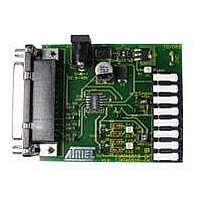
BOARD EVALUATION FOR ATA6826
Manufacturer
Atmel
Specifications of ATA6826-DK
Main Purpose
Power Management, Half H-Bridge Driver (Internal FET)
Embedded
No
Utilized Ic / Part
ATA6826
Primary Attributes
3 Half H-Bridge Drivers, 1A, 2 kV ESD Protection
Secondary Attributes
Short-Circuit, Thermal & Undervoltage Protection
Lead Free Status / RoHS Status
Contains lead / RoHS non-compliant


4. Applications
4.1
8
Demonstration Application
ATA6826
A typical demonstration application consists of a dual full-bridge arrangement with microcontrol-
ler and watchdog to control two DC motors. Such a dual H-bridge arrangement with common
mid-rail allows for independent control of the motors for both directions of rotation. Enter the
appropriate dataword according to
When operating in a safety-critical environment, the use of a separate watchdog IC is recom-
mended (for example, U5021M).
Unlike other circuits of the Atmel driver family, the open-load detection of ATA6826 is active for
all output stages that are currently switched on. If the current through any high-side or low-side
switch does not reach the open-load-detection threshold, an open-load is detected: in the output
register the OPL bit is set to high. The OPL bit is buffered until reset by activation of the SRR bit.
The standby mode is activated by setting the hardware inhibit pin INH to 0V. In this case all out-
puts are switched to tri-state, and any data in the input and output registers is deleted. Switching
pin 10 back to 5V initiates an internal power-on reset.
Short-circuit detection can easily be demonstrated by intentional false activation of the
half-bridge components, for example, HS1 and LS1. This will cause the SCD bit in the output
register to be set. Depending on the OCS bit, the affected outputs are switched off either by
reaching overtemperature or by reaching overcurrent. The corresponding status bits in the out-
put register are set to low. The SCD bit can be reset and the disabled outputs can be re-enabled
by activating the SRR bit. Please note that such activation of SRR just initiates a reset pulse, not
a permanent reset state.
The overtemperature pre-warning is visible at bit TP. While pin CS is set to low, the pre-warning
information is visible in real time at pin DO, because TP is the first bit of the output register. Con-
sequently, the TP bit is not buffered.
As all high-side drivers are internally connected to their low-side counterparts in order to form a
half bridge, switching from HS active to LS active or vice versa with a single programming
sequence could potentially imply some shoot-through current peak across both drivers during
the switching operation. The intelligent internal timing of ATA6826 guarantees that such cross-
over currents are avoided.
Undervoltage detection can be demonstrated with a variable power supply. As soon as the sup-
ply voltage V
output register is set. If the voltage returns to the normal level, the outputs switch on again to
their previous setting. The PSF bit latches the undervoltage occurance and needs to be reset by
SRR activation in the input register.
If the IC is not used in the typical H-bridge arrangement, parallel operation of outputs is possible
for more powerful applications. Two output stages at a time can be paralleled to achieve cur-
rents up to 2A.
In any case, the IC’s maximum power dissipation has to be considered. Excellent thermal con-
tact to an on-board cooling area is obligatory for powerful applications.
VS
falls below threshold, all activated loads are switched off and the PSF bit in the
Table 4-1 on page 9
to set the desired function.
4981A–AUTO–02/07
Related parts for ATA6826-DK
Image
Part Number
Description
Manufacturer
Datasheet
Request
R

Part Number:
Description:
Triple Half-bridge DMOS Output Driver with Serial Input Control
Manufacturer:
ATMEL Corporation
Datasheet:

Part Number:
Description:
MOSFET & Power Driver ICs Triple Half-Bridge Driver
Manufacturer:
Atmel
Datasheet:
Part Number:
Description:
MOSFET & Power Driver ICs Triple Half-Bridge Driver
Manufacturer:
Atmel
Datasheet:

Part Number:
Description:
DEV KIT FOR AVR/AVR32
Manufacturer:
Atmel
Datasheet:
Part Number:
Description:
INTERVAL AND WIPE/WASH WIPER CONTROL IC WITH DELAY
Manufacturer:
ATMEL Corporation
Datasheet:
Part Number:
Description:
Low-Voltage Voice-Switched IC for Hands-Free Operation
Manufacturer:
ATMEL Corporation
Datasheet:
Part Number:
Description:
MONOLITHIC INTEGRATED FEATUREPHONE CIRCUIT
Manufacturer:
ATMEL Corporation
Datasheet:
Part Number:
Description:
AM-FM Receiver IC U4255BM-M
Manufacturer:
ATMEL Corporation
Datasheet:
Part Number:
Description:
Monolithic Integrated Feature Phone Circuit
Manufacturer:
ATMEL Corporation
Datasheet:
Part Number:
Description:
Multistandard Video-IF and Quasi Parallel Sound Processing
Manufacturer:
ATMEL Corporation
Datasheet:
Part Number:
Description:
High-performance EE PLD
Manufacturer:
ATMEL Corporation
Datasheet:
Part Number:
Description:
8-bit Flash Microcontroller
Manufacturer:
ATMEL Corporation
Datasheet: