EVAL-AD7877EBZ Analog Devices Inc, EVAL-AD7877EBZ Datasheet - Page 2
EVAL-AD7877EBZ
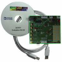
Manufacturer Part Number
EVAL-AD7877EBZ
Description
BOARD EVALUATION FOR AD7877
Manufacturer
Analog Devices Inc
Datasheets
1.AD7877ACBZ-REEL7.pdf
(44 pages)
2.EVAL-AD7877EBZ.pdf
(16 pages)
3.EVAL-AD7877EBZ.pdf
(44 pages)
Specifications of EVAL-AD7877EBZ
Main Purpose
Interface, Touch Screen Controller
Embedded
No
Utilized Ic / Part
AD7877
Primary Attributes
4-Wire Resistive Touch Screen Controller, SPI Interface, On-Chip: Temp Sensor, Voltage Reference, 8-Bit DAC
Secondary Attributes
USB GUI, LCD Noise Reduction Feature, 2.7 ~ 5.25 V, Wake Up on Touch Feature
Lead Free Status / RoHS Status
Lead free / RoHS Compliant


AD7877
TABLE OF CONTENTS
Features .............................................................................................. 1
Applications ....................................................................................... 1
Functional Block Diagram .............................................................. 1
General Description ......................................................................... 1
Revision History ............................................................................... 2
Specifications ..................................................................................... 3
Absolute Maximum Ratings ............................................................ 6
Pin Configurations and Function Descriptions ........................... 7
Typical Performance Characteristics ............................................. 9
Terminology .................................................................................... 13
Circuit Information ........................................................................ 14
REVISION HISTORY
9/09—Rev. B to Rev. C
Changes to Offset Error and Gain Error Parameters .................. 3
Added V
Changes to Pin 23 Description ....................................................... 7
Changes to Power Management (Control Register 2,
Bits[7:6]) Section ............................................................................ 22
Changes to Bit 7 Description (Table 17) ...................................... 36
Updated Outline Dimensions ....................................................... 44
Changes Ordering Guide ............................................................... 44
6/06—Rev. A to Rev. B
Added Wafer Level Chip Scale Package ........................... Universal
Changes to Table 3 ............................................................................ 6
Changes to Figure 21 ...................................................................... 11
Change to Figure 25 ....................................................................... 12
Timing Specifications .................................................................. 5
Timing Diagrams .......................................................................... 5
ESD Caution .................................................................................. 6
Touch Screen Principles ............................................................ 14
Measuring Touch Screen Inputs ............................................... 15
Touch-Pressure Measurement .................................................. 16
STOPACQ Pin ............................................................................ 16
Temperature Measurement ....................................................... 17
Battery Measurement ................................................................. 18
Auxiliary Inputs .......................................................................... 19
Limit Comparison ...................................................................... 19
BAT
to GND Parameter ...................................................... 6
Rev. C | Page 2 of 44
Control Registers ............................................................................ 20
8-Bit DAC ........................................................................................ 26
Serial Interface ................................................................................ 28
General-Purpose I/O Pins ............................................................. 30
Grounding and Layout .................................................................. 32
Register Maps .................................................................................. 33
Detailed Register Descriptions ..................................................... 35
Outline Dimensions ....................................................................... 44
Changes to Figure 38 and Figure 39............................................. 23
Change to Figure 40 ....................................................................... 24
Changes to Data Available Output ( DAV ) Section .................... 24
Updated Outline Dimensions ....................................................... 42
Changes to Ordering Guide .......................................................... 42
11/04—Rev. 0 to Rev. A
Changes to Absolute Maximum Ratings ....................................... 6
Changes to Figure 4 ........................................................................... 7
Changes to Table 4 ............................................................................. 7
Changes to Grounding and Layout section ................................ 32
Changes to Figure 42 ...................................................................... 32
Changes to Ordering Guide .......................................................... 43
7/04—Revision 0: Initial Version
Control Register 1 ...................................................................... 20
Control Register 2 ...................................................................... 21
Sequencer Registers ................................................................... 22
Interrupts ..................................................................................... 24
Syncronizing the AD7877 to the Host CPU ........................... 25
Writing Data ............................................................................... 28
Write Timing ............................................................................... 29
Reading Data ............................................................................... 29
V
GPIO Configuration .................................................................. 30
PCB Design Guidelines for Chip Scale Packages ................... 32
GPIO Registers ........................................................................... 42
Ordering Guide .......................................................................... 44
DRIVE
Pin ..................................................................................... 29
Related parts for EVAL-AD7877EBZ
Image
Part Number
Description
Manufacturer
Datasheet
Request
R


Part Number:
Description:
BOARD EVAL FOR SI270X-A
Manufacturer:
Silicon Laboratories Inc
Datasheet:

Part Number:
Description:
BUCK CONV REF DESIGN KIT IP1201
Manufacturer:
International Rectifier
Datasheet:
Part Number:
Description:
BOARD DEMO SYNC DUAL BUCK CNVTER
Manufacturer:
International Rectifier
Datasheet:
Part Number:
Description:
BOARD DEMO SYNC BUCK CONVETER
Manufacturer:
International Rectifier
Datasheet:

Part Number:
Description:
EVALBOARD/EB Omnidirectional microphone - Analog
Manufacturer:
Analog Devices
Datasheet:
Part Number:
Description:
EVALBOARD/EB Omnidirectional microphone - Analog
Manufacturer:
Analog Devices
Datasheet:


Part Number:
Description:
BOARD EVAL LED DRIVER LT3756
Manufacturer:
Linear Technology
Datasheet:

Part Number:
Description:
BOARD EVAL FOR AD7741/7742
Manufacturer:
Analog Devices Inc
Datasheet:

Part Number:
Description:
±1.7g Dual-Axis IMEMS Accelerometer Evaluation Board
Manufacturer:
Analog Devices Inc
Datasheet:

Part Number:
Description:
IC MULTIPLIER ANALOG 8-SOIC T/R
Manufacturer:
Analog Devices Inc
Datasheet:

Part Number:
Description:
IC ANALOG MULTIPLIER 8-DIP
Manufacturer:
Analog Devices Inc
Datasheet:
Part Number:
Description:
IC ANALOG MULTIPLIER 8-SOIC
Manufacturer:
Analog Devices Inc
Datasheet:
Part Number:
Description:
IC ANALOG MULTIPLIER 8-DIP
Manufacturer:
Analog Devices Inc
Datasheet: