AD9520-4/PCBZ Analog Devices Inc, AD9520-4/PCBZ Datasheet - Page 12
AD9520-4/PCBZ
Manufacturer Part Number
AD9520-4/PCBZ
Description
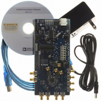
BOARD EVAL FOR AD9520-4
Manufacturer
Analog Devices Inc
Specifications of AD9520-4/PCBZ
Design Resources
Synchronizing Multiple AD9910 1 GSPS Direct Digital Synthesizers (CN0121) Phase Coherent FSK Modulator (CN0186)
Main Purpose
Timing, Clock Generator
Embedded
No
Utilized Ic / Part
AD9520-4
Primary Attributes
1.4 ~ 1.8 GHz Output Frequency
Secondary Attributes
Accepts CMOS, LVDS, or LVPECL References Up to 250 MHz
Silicon Manufacturer
Analog Devices
Application Sub Type
PLL Clock Synthesizer
Kit Application Type
Clock & Timing
Silicon Core Number
AD9520-0, AD9520-2, AD9520-2
Silicon Family Name
AD9520-X
Rohs Compliant
Yes
Lead Free Status / RoHS Status
Lead free / RoHS Compliant


UG-076
OUTPUT DRIVER WINDOW
The output driver window shown in Figure 22 is accessed by
clicking any of the numbered triangular output driver symbols
on the right side of the main window (see Figure 21).
It is important to power down unused outputs on the evaluation
board because they can be a major source of unwanted spurs.
LVPECL and CMOS outputs have different termination require-
ments, and OUT9 through OUT11 have been terminated
differently from OUT0 through OUT8.
Figure 22. Output Driver Window
Figure 21. Driver Symbol
Rev. 0 | Page 12 of 16
OUT 0 through OUT8 are ac-coupled with 200 Ω pull-down
resistors on each output. This termination scheme is ideal for
LVPECL drivers. However, this scheme degrades the CMOS
driver performance. Improved CMOS driver performance is
achieved by removing the 200 Ω pull-down resistors.
OUT9 though OUT11 have no termination resistors, and are
ideally configured for CMOS operation. If you want to use these
drivers in LVPECL mode, pull-down resistors must be added to
the board. If you want to put 50 Ω termination at the SMA
connectors of OUT9 through OUT11, add series decoupling
capacitors so that the termination on OUT9 through OUT11 is
identical to OUT0 through OUT8.
DEBUG WINDOW
The Debug window shown in Figure 23 is accessed by clicking
the Debug option from the View menu.
The Serial I/O section of this window is a convenient way to
read and write registers directly.
Evaluation Board User Guide
Figure 23. Debug Window
Related parts for AD9520-4/PCBZ
Image
Part Number
Description
Manufacturer
Datasheet
Request
R

Part Number:
Description:
12/24 Channel Clock Gen 2,0GH
Manufacturer:
Analog Devices Inc
Datasheet:

Part Number:
Description:
12/24 Channel Clock Gen 2,0GH
Manufacturer:
Analog Devices Inc
Datasheet:
Part Number:
Description:
12/24 Channel Clock Gen 2,0GH
Manufacturer:
Analog Devices Inc
Datasheet:
Part Number:
Description:
12/24 Channel Clock Gen 2,0GH
Manufacturer:
Analog Devices Inc
Datasheet:
Part Number:
Description:
12/24 Channel Clock Gen 2,0GH
Manufacturer:
Analog Devices Inc
Datasheet:
Part Number:
Description:
Clock IC With 2.8GHz On-chip VCO
Manufacturer:
Analog Devices Inc
Datasheet:
Part Number:
Description:
Lock IC With 2.8GHz On-chip VCO
Manufacturer:
Analog Devices Inc
Datasheet:
Part Number:
Description:
12/24 Channel Clock Gen 2,5 GHz VCO
Manufacturer:
Analog Devices Inc
Datasheet:
Part Number:
Description:
12/24 Channel Clock Distribution W/ On-C
Manufacturer:
Analog Devices Inc
Datasheet:
Part Number:
Description:
12/24 Channel Clock Gen 2,25GH
Manufacturer:
Analog Devices Inc
Datasheet:
Part Number:
Description:
12/24 Channel Clock Distribution W/ On-C
Manufacturer:
Analog Devices Inc
Datasheet:
Part Number:
Description:
12/24 Channel Clock Distribution W/ On-C
Manufacturer:
Analog Devices Inc
Datasheet:
Part Number:
Description:
Clock IC With 1.6GHz On-chip VCO
Manufacturer:
Analog Devices Inc
Datasheet:
Part Number:
Description:
Clock IC With 1.6GHz On-chip VCO
Manufacturer:
Analog Devices Inc
Datasheet:
Part Number:
Description:
12/24-Output Clock Generator
Manufacturer:
Analog Devices Inc
Datasheet: