AD9520-4/PCBZ Analog Devices Inc, AD9520-4/PCBZ Datasheet - Page 3
AD9520-4/PCBZ
Manufacturer Part Number
AD9520-4/PCBZ
Description
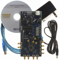
BOARD EVAL FOR AD9520-4
Manufacturer
Analog Devices Inc
Specifications of AD9520-4/PCBZ
Design Resources
Synchronizing Multiple AD9910 1 GSPS Direct Digital Synthesizers (CN0121) Phase Coherent FSK Modulator (CN0186)
Main Purpose
Timing, Clock Generator
Embedded
No
Utilized Ic / Part
AD9520-4
Primary Attributes
1.4 ~ 1.8 GHz Output Frequency
Secondary Attributes
Accepts CMOS, LVDS, or LVPECL References Up to 250 MHz
Silicon Manufacturer
Analog Devices
Application Sub Type
PLL Clock Synthesizer
Kit Application Type
Clock & Timing
Silicon Core Number
AD9520-0, AD9520-2, AD9520-2
Silicon Family Name
AD9520-X
Rohs Compliant
Yes
Lead Free Status / RoHS Status
Lead free / RoHS Compliant


Evaluation Board User Guide
EVALUATION BOARD HARDWARE
The following instructions are for setting up the physical
connections to the AD9520 evaluation board.
When connecting the evaluation board to a PC for the first
time, the user must install the evaluation software prior to
connecting the evaluation board.
POWER AND PC CONNECTIONS
1.
2.
3.
4.
Refer to the Evaluation Board Software section for details on
running the AD9520 evaluation board software.
If the USBSTAT LED is not blinking, ensure that:
•
•
•
SIGNAL CONNECTIONS
To connect signals, connect a signal generator to the J10 SMA
connector. By default, the reference inputs on this evaluation
board are ac-coupled and terminated 50 Ω to ground. An
amplitude setting of 0 dBm to 6 dBm is fine.
If the user wishes to connect a signal to REF2, connect that
signal to the J13 SMA connector. DC-coupling is recommended
in applications requiring automatic hitless reference switching.
There is a possibility that the AD9520 receive buffer can chatter
when an ac-coupled clock stops toggling.
Install AD9520 evaluation software. Administrative
privileges are required for installation. The 64-bit versions
of Windows® are not supported.
Connect the wall power supply to the main power
connector labeled P2. The following five LEDs should be
on: CR1 (USBSTAT), CR7 (VS), CR8 (VS-CP), CR9
(VS_USB), and CR10 (VS_LVPECL).
Connect the USB cables to the evaluation board and the
computer. The red LED labeled CR2 (VBUS) on the
AD9520 evaluation board should illuminate and the CR1
(USBSTAT) LED should start blinking.
If the Found New Hardware Wizard window
automatically appears when the evaluation board is
connected, select Install the software automatically
and click Next.
The Found New Hardware Wizard window may appear
twice, and a system restart may be required.
Jumpers are installed on Position S1 and on the SPI
position of S2.
The jumper on S4 is across the center pin and the minus
symbol.
The USB port on the PC is operational and that the USB
cable is not damaged.
Rev. 0 | Page 3 of 16
Connect an oscilloscope, spectrum analyzer, or other lab
equipment to any of the J0 to J9 SMA connectors on the right
side of the board.
OUT0 through OUT8 are ac-coupled LVPECL outputs.
OUT9 through OUT11 are dc-coupled and have no output
termination. These are intended to allow the user to evaluate
the AD9520 output driver in CMOS mode. To use OUT9
through OUT11 in LVPECL mode, replace the 0 Ω resistors
with 0.1 μF capacitors, and install 200 Ω pull-down resistors.
BYPASSING THE WALL POWER SUPPLY
To bypass the wall power supply, remove the following ferrite
beads (on the backside of the board) : F7, F4, F2, and F6. Next,
connect a bench power supply to TB1 on the evaluation board.
This is useful for making AD9520 power consumption
measurements.
BYPASSING THE PLL (CLOCK DISTRIBUTION ONLY)
To bypass the PLL, connect a signal generator to the SMA connec-
tor labeled CLK. By default, this connection is ac-coupled to
the CLK pin, and terminated with 50 Ω to ground. Refer to the
Evaluation Software Components section for details on running
the AD9520 evaluation board software.
USING AN EXTERNAL VCXO
To use an external VCXO,
1.
2.
3.
USING I
To use I
1.
2.
3.
4.
5.
Install a 0 Ω resistor at R9 and remove R8.
Connect a loop filter and external VCO/VCXO input to J12.
Connect the external VCO/VCXO output to the J11 SMA
connector (CLK input).
Move Jumper S2 to the center and left (I
Move Jumper W1 to the center and left (I
Select the desired I
Jumper S6. Note that S5 = S6 = high is reserved for
SPI mode.
On the evaluation software, select Configure Serial Port
from the I/O menu (see Figure 24).
Click Reset Serial Port, and then click Detect Current
Configuration. A dialog box appears and acknowledges
the I
2
C serial port mode,
2
2
C mode and address.
C SERIAL PORT MODE
2
C address using Jumper S5 and
2
C) pins.
2
C) pins.
UG-076
Related parts for AD9520-4/PCBZ
Image
Part Number
Description
Manufacturer
Datasheet
Request
R

Part Number:
Description:
12/24 Channel Clock Gen 2,0GH
Manufacturer:
Analog Devices Inc
Datasheet:

Part Number:
Description:
12/24 Channel Clock Gen 2,0GH
Manufacturer:
Analog Devices Inc
Datasheet:
Part Number:
Description:
12/24 Channel Clock Gen 2,0GH
Manufacturer:
Analog Devices Inc
Datasheet:
Part Number:
Description:
12/24 Channel Clock Gen 2,0GH
Manufacturer:
Analog Devices Inc
Datasheet:
Part Number:
Description:
12/24 Channel Clock Gen 2,0GH
Manufacturer:
Analog Devices Inc
Datasheet:
Part Number:
Description:
Clock IC With 2.8GHz On-chip VCO
Manufacturer:
Analog Devices Inc
Datasheet:
Part Number:
Description:
Lock IC With 2.8GHz On-chip VCO
Manufacturer:
Analog Devices Inc
Datasheet:
Part Number:
Description:
12/24 Channel Clock Gen 2,5 GHz VCO
Manufacturer:
Analog Devices Inc
Datasheet:
Part Number:
Description:
12/24 Channel Clock Distribution W/ On-C
Manufacturer:
Analog Devices Inc
Datasheet:
Part Number:
Description:
12/24 Channel Clock Gen 2,25GH
Manufacturer:
Analog Devices Inc
Datasheet:
Part Number:
Description:
12/24 Channel Clock Distribution W/ On-C
Manufacturer:
Analog Devices Inc
Datasheet:
Part Number:
Description:
12/24 Channel Clock Distribution W/ On-C
Manufacturer:
Analog Devices Inc
Datasheet:
Part Number:
Description:
Clock IC With 1.6GHz On-chip VCO
Manufacturer:
Analog Devices Inc
Datasheet:
Part Number:
Description:
Clock IC With 1.6GHz On-chip VCO
Manufacturer:
Analog Devices Inc
Datasheet:
Part Number:
Description:
12/24-Output Clock Generator
Manufacturer:
Analog Devices Inc
Datasheet: