CDB5376 Cirrus Logic Inc, CDB5376 Datasheet
CDB5376
Specifications of CDB5376


Related parts for CDB5376


CDB5376 Summary of contents
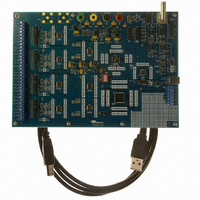
Page 1
Low-noise, Programmable Gain, Differential Amplifier Features & Desription Signal Bandwidth kHz Selectable Gain: x1, x2, x4, x8, x16, x32, x64 Differential Inputs, Differential Outputs • Multiplexed inputs: INA, INB, 800Ω termination • Rough / fine outputs for ...
Page 2
TABLE OF CONTENTS 1. CHARACTERISTICS AND SPECIFICATIONS .............................................................................. 3 SPECIFIED OPERATING CONDITIONS ....................................................................................... 3 ABSOLUTE MAXIMUM RATINGS ................................................................................................. 3 TEMPERATURE CONDITIONS .................................................................................................... 3 ANALOG CHARACTERISTICS ..................................................................................................... 4 DIGITAL CHARACTERISTICS ...................................................................................................... 7 POWER SUPPLY CHARACTERISTICS ........................................................................................ 8 2. GENERAL DESCRIPTION ............................................................................................................. ...
Page 3
CHARACTERISTICS AND SPECIFICATIONS • Min / Max characteristics and specifications are guaranteed over the • Typical performance characteristics and specifications are measured at nominal supply voltages and T • GND = 0 V. Single-ended voltages with respect to GND, ...
Page 4
ANALOG CHARACTERISTICS Parameter Noise Performance Input Voltage Noise f Input Voltage Noise Density f Input Current Noise Density Distortion Performance Total Harmonic Distortion (Note 5) Linearity (Note 5) Notes: 4. Guaranteed by design and/or characterization. 5. Tested with a full ...
Page 5
ANALOG CHARACTERISTICS (CONT.) Parameter Gain Gain, Differential Gain, Common Mode Gain Accuracy, Absolute Gain Accuracy, Relative Gain Drift Offset Offset Voltage, Input Referred Offset After Calibration, Absolute Offset Calibration Range Offset Voltage Drift 6. Common mode signals pass unchanged through ...
Page 6
ANALOG CHARACTERISTICS (CONT.) Parameter Analog Input Characteristics Input Signal Frequencies Input Voltage Range (Vcm ± Signal) Full Scale Input, Differential Input Impedance, Differential Input Impedance, Common Mode Input Bias Current Crosstalk, Multiplexed Inputs Common to Differential Mode Rejection Analog Output ...
Page 7
DIGITAL CHARACTERISTICS Parameter Digital Characteristics High Level Input Drive Voltage Low Level Input Drive Voltage Input Leakage Current Digital Input Capacitance Rise Times, Digital Inputs Except CLK Fall Times, Digital Inputs Except CLK Master Clock Specifications Master Clock Frequency Master ...
Page 8
POWER SUPPLY CHARACTERISTICS Parameter Power Supply Current, Normal Analog Power Supply Current Digital Power Supply Current Power Supply Current, Power Down (PWDN=1) Analog Power Supply Current Digital Power Supply Current Power Supply Rejection Power Supply Rejection Ratio Notes: 17. All ...
Page 9
GENERAL DESCRIPTION The CS3301A is a low-noise chopper-stabilized CMOS differential input, differential output ampli- fier for precision analog signals between DC and 2 kHz. It has multiplexed inputs, rough / fine out- puts and programmable gains of x1, x2, ...
Page 10
Differential M Sensor U X 2.1.3 Differential Signals Analog signals into and out of the CS3301A are differential, consisting of two halves with equal but opposite magnitude varying about a common mode voltage. A full scale 5 Vpp differential signal ...
Page 11
MUX0 and MUX1 pins as shown in Table 1 on page 7. Although a mux selection is provided to enable the INA and INB switches simultaneously, signal cur- rent should not be driven through them in this ...
Page 12
Connection Diagram Figure 5 on page 12 shows a connection diagram for the CS3301A amplifier when used with the CS5372A dual ∆Σ modulator, the CS4373A Test DAC, and the CS5376A digital filter. The diagram 3 GAIN VA+ VA+ 0.1µF ...
Page 13
PIN DESCRIPTION Positive Analog Power Supply Negative Analog Rough Output Negative Analog Fine Output Negative Analog Power Supply Non-Inverting Input A Inverting Input A Inverting Input B Non-Inverting Input B Test Mode Output Positive Analog Fine Output Positive Analog ...
Page 14
PACKAGE DIMENSIONS 24 PIN SSOP PACKAGE DRAWING TOP VIEW DIM ∝ Notes: 1. “D” and “E1” are reference datums and do not included mold flash ...
Page 15
ORDERING INFORMATION Model CS3301A-IS CS3301A-ISZ (lead free) 6. ENVIRONMENTAL, MANUFACTURING, & HANDLING INFORMATION Model Number CS3301A-IS CS3301A-ISZ (lead free) * MSL (Moisture Sensitivity Level) as specified by IPC/JEDEC J-STD-020. DS757F1 Temperature -40 to +85 °C Peak Reflow Temp MSL ...
Page 16
REVISION HISTORY Revision Date PP1 FEB 2007 F1 MAR 2007 Contacting Cirrus Logic Support For all product questions and inquiries contact a Cirrus Logic Sales Representative. To find one nearest you go to www.cirrus.com IMPORTANT NOTICE Cirrus Logic, Inc. ...