CDB5376 Cirrus Logic Inc, CDB5376 Datasheet
CDB5376
Specifications of CDB5376


Related parts for CDB5376


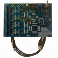
CDB5376 Summary of contents
Page 1
Low-power, Multi-channel Decimation Filter Features 1- to 4-channel Digital Decimation Filter Multiple On-chip FIR and IIR Coefficient Sets Programmable Coefficients for Custom Filters Synchronous Operation Selectable Output Word Rate 4000, 2000, 1000, 500, 333, 250 SPS 200, 125, 100, 50, ...
Page 2
TABLE OF CONTENTS 1. General Description . . . . . . . . . . . . . . . . . . . . . . . . . . . . . . . . . . ...
Page 3
Pin Descriptions . . . . . . . . . . . . . . . . . . . . . . . . . . . . . . . . . . . . . ...
Page 4
TBS Synchronization . . . . . . . . . . . . . . . . . . . . . . . . . . . . . . . . . . . . . ...
Page 5
Figure 14. EEPROM Configuration Block Diagram . . . . . . . . . . . . . . . . . . . . . .26 Figure 15. SPI 1 EEPROM Read Transactions . . . . . ...
Page 6
LIST OF TABLES Table 1. Microcontroller and EEPROM Configuration Commands . . . . . . . . . . .10 Table 2. TBS Configurations Using On-Chip Data . . . . . . . . . . . . ...
Page 7
Serial Data Output Port JTAG Interface 1. GENERAL DESCRIPTION The CS5376A is a multi-channel digital filter with integrated system peripherals. Figure 1 illustrates a simplified block diagram of the CS5376A. 1.1 Digital Filter Features • Multi-channel decimation CS5371A/72A ∆Σ modulators. ...
Page 8
Modulator Sinc Filter Input 2 - 64000 512 kHz Gain & DC Offset Corrections • Digital offset correction and calibration. - Individual channel offset correction to re- move measurement offsets. - Calibration engine for automatic calcula- tion of offset correction ...
Page 9
SPS (9.25 mW/channel). 40 µW standby mode. - • Flexible power supply configurations. - Separate digital logic core, telemetry I/O, and modulator I/O power supplies. - Telemetry I/O and modulator I/O interfaces ...
Page 10
Microcontroller Boot Configuration Commands Name NOP WRITE DF REGISTER READ DF REGISTER WRITE FIR COEFFICIENTS WRITE IIR COEFFICIENTS WRITE ROM COEFFICIENTS WRITE TBS DATA WRITE ROM TBS FILTER START FILTER STOP EEPROM Boot Configuration Commands Name NOP WRITE DF REGISTER ...
Page 11
Bits 23:20 Selection 0000 Bits 15:12 IIR2 Coefficients 0000 2000 SPS 0001 1000 SPS 0010 500 SPS 0011 333 SPS 0100 250 SPS Figure 3. ...
Page 12
SPI 1 Registers Name Addr. SPI1CTRL SPI1CMD SPI1DAT1 SPI1DAT2 Digital Filter Registers Name Addr. CONFIG 00 RESERVED 01-0D GPCFG0 0E GPCFG1 0F SPI2CTRL 10 SPI2CMD 11 SPI2DAT 12 ...
Page 13
CHARACTERISTICS AND SPECIFICATIONS • Min / Max characteristics and specifications are guaranteed over the Specified Operating Conditions. • Typical performance characteristics and specifications are derived from measurements taken at nomi- nal supply voltages and T A • GND, GND1, ...
Page 14
THERMAL CHARACTERISTICS Parameter Allowable Junction Temperature Junction to Ambient Thermal Impedance Ambient Operating Temperature (Power Applied) DIGITAL CHARACTERISTICS Parameter High-Level Input Drive Voltage Low-Level Input Drive Voltage High-Level Output Drive Voltage Low-Level Output Drive Voltage Rise Times, Digital Inputs Fall ...
Page 15
SWITCHING CHARACTERISTICS SPI 1 Interface Timing (External Master) SSI MOSI MSB t 1 SCK1 SCLK SS I MISO MSB SCK1 SCLK Parameter MOSI Write Timing SSI Enable to Valid Latch Clock Data Set-up Time Prior to SCK1 Rising Data Hold ...
Page 16
SWITCHING CHARACTERISTICS Serial Data Port (SD Port) SDRDY SDCLK t 3 SDDAT SDTKI t 1 SDTKO t 2 Parameter SDTKI to SDRDY Falling Edge SDTKI High Time Width SDRDY Falling Edge to SDCLK Falling Edge Data ...
Page 17
SWITCHING CHARACTERISTICS CLK, SYNC, MCLK, MSYNC, and MDATAx SYNC MCLK MSYNC MDATAx Note: SYNC input latched on MCLK rising edge. MSYNC output triggered by MCLK falling edge. f MCLK msd MCLK msh MCLK Figure ...
Page 18
SWITCHING CHARACTERISTICS Test Bit Stream (TBS) TBSCLK TBSDATA MCLK Note: Example timing shown for a 256 kHz output rate and no programmable delays. Parameter TBS Clock Timing TBS Clock Period TBS Clock High Time TBS Clock Low Time TBS Data ...
Page 19
Geophone or Hydrophone Sensor Geophone or Hydrophone Sensor Geophone or Hydrophone Sensor Geophone or Hydrophone Sensor 3. SYSTEM DESIGN WITH CS5376A Figure 9 illustrates a simplified block diagram of the CS5376A in a multi-channel measurement sys- tem four ...
Page 20
Clock Generation A single 32.768 MHz low-jitter clock input, which can be generated from a VCXO based PLL, is re- quired to drive the CS5376A device. Clock inputs for other system devices are driven by clock out- puts from ...
Page 21
TBSCLK TBSDATA MCLK/2 MSYNC MDATA4 MFLAG4 4. POWER SUPPLIES The CS5376A has three sets of power supply in- puts. Two sets supply power to the I/O pins of the device (VDD1, VDD2), and the third supplies power to the logic ...
Page 22
VD, GND - Pins 7, 40, 6, 23, 39 Sets the operational voltage of the CS5376A logic core. Can be driven with voltages from supply minimizes total power consumption. 4.2 Bypass Capacitors ...
Page 23
RESET 5. RESET CONTROL The CS5376A reset signal is active low. When re- leased, a series of self-tests are performed and the device either actively boots from an external EE- PROM or enters an idle state waiting for microcon- troller ...
Page 24
CLK 6. CLOCK GENERATION The CS5376A requires a 32.768 MHz master clock input, which is used to generate internal digital fil- ter clocks and external modulator clocks. 6.1 Pin Description CLK - Pin 58 Clock input, nominal frequency 32.768 MHz. ...
Page 25
SYNC 1 MSEN 7. SYNCHRONIZATION The CS5376A has a dedicated SYNC input that aligns the internal digital filter phase and generates an external signal for synchronizing modulator an- alog sampling. By providing simultaneous rising edges to the SYNC pins ...
Page 26
Figure 14. EEPROM Configuration Block Diagram 8. CONFIGURATION BY EEPROM After reset, the CS5376A reads the state of the BOOT pin to determine a source for configuration commands. If BOOT is high, the CS5376A ini- tiates serial transactions through the ...
Page 27
Instruction Opcode Read 0x03 SPI 1 Read from EEPROM SSI MOSI MISO EECS Cycle SCK1 MSB MOSI MSB MISO EECS DS612F4 Address ADDR[15:0] Read data beginning at the address given in ADDR. READ 2 BYTE CMD ADDR 0x03 ADDR ADDR ...
Page 28
Mfg Header 0010h 8-bit Command N x 24-bit Data 8-bit Command N x 24-bit Data . . . 1FFFh Figure 16. 8 Kbyte EEPROM Memory Organization 5 KByte (40 Kbit), which includes command over- head: Memory Requirement Digital Filter ...
Page 29
Sample Command: Write IIR1 coefficients 0x84BC9D, 0x7DA1B1, 0x825E4F, and IIR2 coefficients 0x83694F, 0x3CAD5F, 0x3E5104, 0x835DF8, 0x3E5104 ...
Page 30
Sample Command: Write test bit stream data 0x000000, 0x0007DA, 0x000FB5, 0x00178F Write TBS ROM Data - 0x06 This EEPROM command selects the on-chip test ...
Page 31
Addr Data Description 00 00 Mfg header Write ...
Page 32
Digital Filter Command Interpreter Figure 17. Serial Peripheral Interface 1 (SPI 1) Block Diagram 9. CONFIGURATION BY MICROCONTROLLER After reset, the CS5376A reads the state of the BOOT pin to determine a source for configuration commands. If BOOT is low, ...
Page 33
Instruction Opcode Write 0x02 Read 0x03 Microcontroller Write to SPI 1 SSI MOSI MISO Microcontroller Read from SPI 1 SSI MOSI MISO Cycle SCK1 MSB MOSI MSB MISO SSI DS612F4 Address ADDR[7:0] Write SPI 1 registers beginning at the address ...
Page 34
SPI 1 registers The SPI 1 registers are shown in Figure 19 and are 24-bit registers mapped into an 8-bit register space as high, mid, and low bytes. See “SPI 1 Registers” on page 81 for the bit definitions ...
Page 35
The E2DREQ bit reads high while a configuration command is being processed. When low, the digital filter is ready to receive a new configuration com- mand. 9.4 Microcontroller Configuration Commands A summary of available microcontroller configura- tion commands is listed ...
Page 36
Delay 1 ms, monitor SINT, or poll E2DREQ MOSI MISO Delay 1 ms, monitor SINT, or poll E2DREQ MOSI ...
Page 37
Sample Command: Write test bit stream data 0x000000, 0x0007DA, 0x000FB5, 0x00178F Delay 1 ms, monitor SINT, or poll E2DREQ ...
Page 38
Transaction DS612F4 SPI Data Delay 1ms, monitor SINT, or poll E2DREQ Delay 1ms, monitor ...
Page 39
MCLK / MCLK MCLK/2 MSYNC MSYNC Generate MDI Input MDATA[4:1] MFLAG[4:1] 512 kHz DC Offset & Gain Correction 10.MODULATOR INTERFACE The CS5376A performs digital filtering for up to four ∆Σ modulators. Signals from the modulators are connected through the modulator ...
Page 40
Modulator Data Inputs The MDATA input expects 1-bit ∆Σ data at a 512 kHz or 256 kHz rate. The input rate is selected by a bit in the CONFIG register (0x00). By default, MDATA is expected at 512 kHz. ...
Page 41
Modulator SINC Filter Input 2 - 64000 512 kHz DC Offset & Gain Correction 11.DIGITAL FILTER INITIALIZATION The CS5376A digital filter consists of three multi- stage sections: a three stage SINC filter, a two stage FIR filter, and a two ...
Page 42
Bits 23:20 Selection 0000 Bits 15:12 IIR2 Coefficients 0000 2000 SPS 0001 1000 SPS 0010 500 SPS 0011 333 SPS 0100 250 SPS Figure 22. ...
Page 43
Input 4th order 4th order sinc3 sinc3 stage1 stage2 5 12.SINC FILTER The SINC filters primary purpose is to attenuate out-of-band noise components from the ∆Σ modu- lators. While doing so, they decimate 1-bit ...
Page 44
SINC1 – Single stage, fixed decimate order decimate coefficients SINC2 – Multi-stage, variable decimation Stage 1: 4 Stage 2: 4 Stage 3: 5 Stage 4: 6 SINC3 – Multi-stage, variable decimation Stage 1: ...
Page 45
Filter Type SINC1 th 5 order decimate coefficients Filter Type SINC2 (Stage 1) SINC2 (Stage order decimate coefficients SINC2 (Stage order decimate coefficients SINC2 (Stage ...
Page 46
Filter Type SINC3 (Stage 1) SINC3 (Stage 2) SINC3 (Stage order decimate coefficients SINC3 (Stage order decimate coefficients SINC3 (Stage order decimate ...
Page 47
FIR1 Filter - decimate by 4 13.FIR FILTER The finite impulse response (FIR) filter block con- sists of two cascaded stages, FIR1 and FIR2. It compensates for SINC filter droop and creates a low-pass corner to block aliased components of ...
Page 48
Programmable FIR Coefficients A maximum of 255 + 255 coefficients can be pro- grammed into FIR1 and FIR2 to create a custom filter response. The total number of coefficients for the FIR filter is fundamentally limited by the avail- ...
Page 49
FIR1 – Single stage, fixed decimate by 4 Coefficient set 0: linear phase decimate coefficients Coefficient set 1: minimum phase decimate coefficients SINC droop compensation filter FIR2 – Single stage, fixed decimate by 2 ...
Page 50
Individual filter stage group delay (no IIR) SINC1 SINC2 Stage 4 Stages 3,4 Stages 2,3,4 Stages 1,2,3,4 SINC3 Stage 6 Stage 5 Stages 4,5 Stages 3,4,5 Stages 2,3,4,5 Stages 1,2,3,4,5 FIR1 Coefficient Set 0 Coefficient Set 1 FIR2 Coefficient Set ...
Page 51
Minimum phase group delay FIR1 Minimum Phase Group Delay (Normalized frequency) FIR2 Minimum Phase Group Delay (Normalized frequency) DS612F4 Figure 27. Minimum Phase Group Delay CS5376A 51 ...
Page 52
Filter Type FIR1 (Coefficient set 0) Low pass, SINC compensation Linear phase decimate coefficients FIR1 (Coefficient set 1) Low pass, SINC compensation Minimum phase decimate coefficients DS612F4 Filter Coefficients (normalized 24-bit 558 ...
Page 53
Filter Type FIR2 (Coefficient set 0) Low pass, passband to 40% f Linear phase decimate by 2 126 coefficients DS612F4 Filter Coefficients (normalized 24-bit - -371 -870 -986 ...
Page 54
Filter Type FIR2 (Coefficient set 1) Low pass, passband to 40% f Minimum phase decimate by 2 126 coefficients DS612F4 Filter Coefficients (normalized 24-bit 4019 43275 235427 848528 ...
Page 55
Order IIR1 -a 11 3rd Order IIR3 implemented by running both IIR1 and IIR2 stages 14.IIR FILTER The infinite impulse response (IIR) filter block consists of two cascaded stages, IIR1 and IIR2. It creates a high-pass corner to block ...
Page 56
IIR filter with unnormalized coefficients (-a21 * W4) + (-a22 * W5 (W3 * b20) + (W4 * b21) ...
Page 57
IIR1 – Single stage, no decimation st 1 order no decimation, 3 coefficients Coefficient set 0: high-pass, corner 0.15% f Coefficient set 1: high-pass, corner 0.30% f Coefficient set 2: high-pass, corner 0.60% f Coefficient set 3: high-pass, corner 0.90% ...
Page 58
Filter Type IIR1 (Coefficient set order, high pass Corner at 0.15 coefficients IIR1 (Coefficient set order, high pass Corner at 0.30 coefficients IIR1 (Coefficient set ...
Page 59
MDI Input 512 kHz 4 Offset Gain Correction 4 Correction Offset Calibration 4 15.GAIN AND OFFSET CORRECTION The CS5376A digital filter can apply independent gain and offset corrections to the data of each mea- surement channel. Also, an offset calibration ...
Page 60
OFFSETx registers (0x25-0x28) from the digital filter output data word. Offset correction values are 24-bit two’s comple- ment with a maximum positive value of 0x7FFFFF, and a maximum negative value of 0x800000. If ap- plying an offset ...
Page 61
System Telemetry Token Out Data Ready Clock Out Data In Token In 16.SERIAL DATA PORT Once digital filtering is complete, each 24-bit out- put sample is combined with an 8-bit status byte. These 32-bit data words are written to an ...
Page 62
Word 1 Status Data MFLAG -- Modulator Modulator Error BRK digital filter register (0x29) programs the sample delay for the TB bit output. See “Time Break Controller” on page 67 for more information ...
Page 63
SDTKI SDTKO SDRDY SDCLK SDDAT data is read from the SD port data FIFO, SDRDY is released and SDTKO is pulsed high for 100 nS. 16.3.2 Continuous Mode To have the CS5376A automatically initiate SD port transactions whenever data becomes ...
Page 64
Figure 34. Test Bit Stream Generator Block Diagram 17.TEST BIT STREAM GENERATOR The CS5376A test bit stream (TBS) generator cre- ates sine wave ∆Σ bit stream data to drive an exter- nal test DAC. The TBS digital output can also ...
Page 65
Test Bit Stream Characteristic Equation: (Signal Freq TBS Data) * (Interpolation + 1) = Output Rate Example: (31.25 Hz) * (1024) * (0x07 + 1) = 256 kHz Signal Frequency (TBSDATA) 10.00 Hz 10.00 Hz 25.00 Hz 25.00 ...
Page 66
CS5376A. The number of data points to write maximum of 1024, depends on the required test signal frequency, out- put rate, and available interpolation factors. Cus- tom data sets must be ...
Page 67
TIMEB 18.TIME BREAK CONTROLLER A time break signal is used to mark timing events that occur during measurement. An external signal sets a flag in the status byte of an output sample to mark when the external event occurred. A ...
Page 68
CS output from SPI Data bit 19.GENERAL PURPOSE I/O The General Purpose I/O (GPIO) block provides 12 general purpose pins to interface with external hardware. 19.1 Pin Descriptions GPIO[4:0]:CS[4:0] - Pins Standard GPIO pins also used as ...
Page 69
Any GPIO pin can be used as an open-drain output by setting the data value to 0, enabling the pull-up, and using the GP_DIR direction bits to control the pin value. This open-drain output configuration uses the internal pull-up resistor ...
Page 70
Digital Filter Figure 37. Serial Peripheral Interface 2 (SPI 2) Block Diagram 20.SERIAL PERIPHERAL INTERFACE 2 The Serial Peripheral Interface 2 (SPI 2) port is a master mode SPI port designed to interface with se- rial peripherals. By writing the ...
Page 71
SPI 2 Control Register The SPI 2 hardware is configured by the SPI2CTRL digital filter register (0x10). Bits in this register select the serial input pin and chip select pin used for a transaction, set the total number of ...
Page 72
During a transaction, bits in SPI2CMD are output MSB first, with data in SPI2DAT written or read following. 20.3.3 SPI 2 Data Register The SPI2DAT register (0x12 24-bit digital fil- ter register containing three SPI data bytes. Data ...
Page 73
Instruction Opcode Write 0x02 Read 0x03 SPI 2 Write to External Slave SPI 2 Read from External Slave SPI modes 1 and 4 work similarly to modes 0 and 3, with the serial clock ...
Page 74
SPI 2 Transaction with SCKPH=0 Cycle 1 SCK2 SCKPO = 0 SCK2 SCKPO = 1 SO MSB SI MSB Slave devices only drive SI after being selected and responding to a read command. CS SPI 2 Transaction with SCKPH=1 Cycle ...
Page 75
TRST TMS TCK TDI 21.BOUNDARY SCAN JTAG The CS5376A includes an IEEE 1149.1 boundary scan JTAG port to test PCB interconnections. Refer to the IEEE 1149.1 specification for more information about boundary scan testing. 21.1 Pin Descriptions TRST - Pin ...
Page 76
JTAG Reset As required by the IEEE 1149.1 specification, the JTAG TRST signal is independent of the CS5376A RESET signal. In systems not using the JTAG port, TRST should be connected to ground. In systems using the JTAG port, ...
Page 77
BRC Pin Function 1 TBSCLK data out 2 TBSDATA data out 3 DNC data out 4 MCLK/2 data out 5 MCLK data out 6 MSYNC data out 7 MDATA4 data in 8 MFLAG4 data in 9 MDATA3 data in 10 ...
Page 78
REVISION HISTORY The CS5376A is a pin compatible upgrade to the CS5376. The part family has had three revisions: CS5376 rev A CS5376 rev B CS5376A rev A The part number change for CS5376A reflects ad- ditional functionality built ...
Page 79
Modified SINC2 filter to correct gain and timing errors Corrected SINC2 decimate by 2 gain error which affected 4000 SPS operation. Also mod- ified SINC2 decimate by 16 output timing to match output of other SINC2 rates. Previous SINC2 decimate ...
Page 80
Added Test Bit Stream (TBS) synchroniza- tion in sine wave mode. The TBS sine wave phase will reset if bit 11 of the TBSCFG register is set (TBSCFG bit and a rising edge is received on the ...
Page 81
SUMMARY 23.1 SPI 1 Registers The CS5376A SPI 1 registers interface the serial port to the digital filter. Name Addr. SPI1CTRLH 00 SPI1CTRLM 01 SPI1CTRLL 02 SPI1CMDH 03 SPI1CMDM 04 SPI1CMDL 05 SPI1DAT1H 06 SPI1DAT1M 07 SPI1DAT1L 08 SPI1DAT2H ...
Page 82
SPI1CTRL : 0x00, 0x01, 0x02 Figure 41. SPI 1 Control Register SPI1CTRL (MSB R/W R/W1 R SMODF -- -- R R ...
Page 83
SPI1CMD : 0x03, 0x04, 0x05 Figure 42. SPI 1 Command Register SPI1CMD (MSB S1CMD23 S1CMD22 S1CMD21 R/W R/W R S1CMD15 S1CMD14 S1CMD13 R/W R/W R ...
Page 84
SPI1DAT1 : 0x06, 0x07, 0x08 Figure 43. SPI 1 Data Register SPI1DAT1 (MSB S1DAT23 S1DAT22 S1DAT21 R/W R/W R S1DAT15 S1DAT14 S1DAT13 R/W R/W R ...
Page 85
SPI1DAT2 : 0x09, 0x0A, 0x0B Figure 44. SPI 1 Data Register SPI1DAT2 (MSB S1DAT23 S1DAT22 S1DAT21 R/W R/W R S1DAT15 S1DAT14 S1DAT13 R/W R/W R ...
Page 86
Digital Filter Registers The CS5376A digital filter registers control hardware peripherals and filtering functions. Name Addr. CONFIG 00 RESERVED 01-0D GPCFG0 0E GPCFG1 0F SPI2CTRL 10 SPI2CMD 11 SPI2DAT 12 RESERVED 13-1F FILTCFG 20 GAIN1 21 GAIN2 22 GAIN3 ...
Page 87
CONFIG : 0x00 Figure 45. Hardware Configuration Register CONFIG (MSB) R/W R/W R R/W R/W R MCKEN2 ...
Page 88
GPCFG0 : 0x0E Figure 46. GPIO Configuration Register GPCFG0 (MSB GP_DIR7 GP_DIR6 GP_DIR5 R/W R/W R GP_PULL7 GP_PULL6 GP_PULL5 R/W R/W R GP_DATA7 GP_DATA6 ...
Page 89
GPCFG1 : 0x0F Figure 47. GPIO Configuration Register GPCFG1 (MSB R/W R/W R R/W R/W R ...
Page 90
SPI2CTRL : 0x10 Figure 48. SPI 2 Control Register SPI2CTRL (MSB WOM SCKFS2 SCKFS1 R/W R/W R RCH1 RCH0 D2SOP R/W R DNUM2 ...
Page 91
SPI2CMD : 0x11 Figure 49. SPI 2 Command Register SPI2CMD (MSB R/W R/W R SCMD15 SCMD14 SCMD13 R/W R/W R SCMD7 ...
Page 92
SPI2DAT : 0x12 Figure 50. SPI 2 Data Register SPI2DAT (MSB SDAT23 SDAT22 SDAT21 R/W R/W R SDAT15 SDAT14 SDAT13 R/W R/W R SDAT7 ...
Page 93
FILTCFG : 0x20 Figure 51. Filter Configuration Register FILTCFG (MSB R/W R/W R ORCAL USEOR R/W R/W R DEC3 DEC2 ...
Page 94
GAIN1 - GAIN4 : 0x21 - 0x24 Figure 52. Gain Correction Register GAIN1 (MSB GAIN23 GAIN22 GAIN21 R/W R/W R GAIN15 GAIN14 GAIN13 R/W R/W R ...
Page 95
OFFSET1 - OFFSET4 : 0x25 - 0x28 Figure 53. Offset Correction Register OFFSET1 (MSB OFST23 OFST22 OFST21 R/W R/W R OFST15 OFST14 OFST13 R/W R/W R ...
Page 96
TIMEBRK : 0x29 Figure 54. Time Break Counter Register TIMEBRK (MSB TBRK23 TBRK22 TBRK21 R/W R/W R TBRK15 TBRK14 TBRK13 R/W R/W R TBRK7 ...
Page 97
TBSCFG : 0x2A Figure 55. Test Bit Stream Configuration Register TBSCFG (MSB INTP7 INTP6 INTP5 R/W R/W R RATE2 RATE1 R/W R/W R ...
Page 98
TBSGAIN : 0x2B Figure 56. Test Bit Stream Gain Register TBSGAIN (MSB TGAIN23 TGAIN22 TGAIN21 R/W R/W R TGAIN15 TGAIN14 TGAIN13 R/W R/W R ...
Page 99
SYSTEM1, SYSTEM2 : 0x2C, 0x2D Figure 57. User Defined System Register SYSTEM1 (MSB SYS23 SYS22 SYS21 R/W R/W R SYS15 SYS14 SYS13 R/W R/W R ...
Page 100
VERSION : 0x2E Figure 58. Hardware Version ID Register VERSION (MSB TYPE7 TYPE6 TYPE5 R/W R/W R HW7 HW6 HW5 R/W R/W R ROM7 ...
Page 101
SELFTEST : 0x2F Figure 59. Self Test Result Register SELFTEST (MSB R/W R/W R DRAM3 DRAM2 DRAM1 R/W R/W R DROM3 ...
Page 102
DESCRIPTIONS TIMEB CLK SYNC SDDAT SDRDY SDCLK SDTKO SDTKI TRST TMS 64 1 TCK 2 TDI 3 TDO 4 5 GND TBSCLK 8 9 TBSDATA 10 DNC 11 VDD2 12 13 MCLK/2 14 MCLK 15 MSYNC ...
Page 103
Pin Pin Name Number 1 TRST TMS 2 TCK 3 TDI 4 TDO 5 TBSCLK 8 TBSDATA 9 DNC 10 MCLK/2 12 MCLK 13 MSYNC 14 MDATA[4:1] 15, 17, 19, 21 MFLAG[4:1] 16, 18, 20, 22 SI[4:1] 26, 27, 28, ...
Page 104
Pin Pin Name Number CLK 58 SYNC 59 SDDAT 60 61 SDRDY SDCLK 62 SDTKO 63 SDTKI 64 VDD1 54 VDD2 11 GND1, GND2, GND 6, 23, 24, 38, 39, 53 104 Pin Type Clock and ...
Page 105
DIMENSIONS 64L TQFP PACKAGE DRAWING D1 D ∝ L DIM µ DS612F4 INCHES MIN MAX --- 0.063 0.002 0.006 0.05 0.007 0.011 0.17 0.461 0.484 ...
Page 106
INFORMATION Model CS5376A-IQ CS5376A-IQZ Lead Free 27.ENVIRONMENTAL, MANUFACTURING, & HANDLING INFORMATION Model Number CS5376A-IQ CS5376A-IQZ Lead Free * MSL (Moisture Sensitivity Level) as specified by IPC/JEDEC J-STD-020. 28.REVISION HISTORY Revision Date PP1 SEP 2003 Initial “Preliminary Product” release. F1 ...