CDB5376 Cirrus Logic Inc, CDB5376 Datasheet
CDB5376
Specifications of CDB5376


Related parts for CDB5376


CDB5376 Summary of contents
Page 1
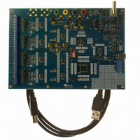
... Time domain analysis – Noise histogram analysis www.cirrus.com General Description The CDB5376 board is used to evaluate the functionality and performance of the Cirrus Logic multichannel seis- mic chip set. Data sheets for the CS3301A, CS3302A, CS4373A, CS5371A/72A, and CS5376A devices should be consulted when using the CDB5376 evaluation board ...
Page 2
... Windows, Windows XP, Windows 2000, and Windows NT are trademarks or registered trademarks of Microsoft Corporation. Intel and Pentium are registered trademarks of Intel Corporation. SPI is a trademark of Motorola, Inc (I2C registered trademark of Philips Semiconductor Corporation. USBExpress is a registered trademark of Silicon Laboratories, Inc. 2 Changes CS3301 to CS3301A CS3302 to CS3302A CS5372 to CS5372A CDB5376 DS612DB3 ...
Page 3
... Default DIP Switch Settings ............................................................................... 10 1.3 Software Setup ................................................................................................................ 11 1.3.1 PC Requirements ................................................................................................ 11 1.3.2 Seismic Evaluation Software Installation ............................................................ 11 1.3.3 USBXpress Driver Installation ............................................................................. 11 1.3.4 Launching the Seismic Evaluation Software ....................................................... 12 1.4 Self-testing CDB5376 ...................................................................................................... 13 1.4.1 Noise test ............................................................................................................ 13 1.4.2 Distortion Test ..................................................................................................... 14 2. HARDWARE DESCRIPTION ................................................................................................. 15 2.1 Block Diagram ................................................................................................................ 15 2.2 Analog Hardware ............................................................................................................. 16 2 ...
Page 4
... Zoom ................................................................................................................... 50 3.4.6 Refresh ................................................................................................................ 50 3.4.7 Harmonics ........................................................................................................... 50 3.4.8 Spot Noise ........................................................................................................... 50 3.4.9 Plot Error ............................................................................................................. 50 3.5 Control Panel ................................................................................................................... 51 3.5.1 DF Registers ....................................................................................................... 52 3.5.2 DF Commands .................................................................................................... 52 3.5.3 SPI ...................................................................................................................... 52 3.5.4 Macros ................................................................................................................ 53 3.5.5 GPIO ................................................................................................................... 53 3.5.6 Customize ........................................................................................................... 54 3.5.7 External Macros .................................................................................................. 54 4. BILL OF MATERIALS ........................................................................................................... 55 5. LAYER PLOTS ...................................................................................................................... 58 6. SCHEMATICS ........................................................................................................................ 66 4 CDB5376 DS612DB3 ...
Page 5
... LIST OF FIGURES Figure 1. CDB5376 Block Diagram ............................................................................................... 15 Figure 2. RC Filter External Components ..................................................................................... 20 Figure 3. CPLD Default Signal Assignments ................................................................................ 26 Figure 4. Differential Pair Routing ................................................................................................. 35 Figure 5. Quad Group Routing...................................................................................................... 36 Figure 6. Bypass Capacitor Placement......................................................................................... 36 Figure 7. Dual-row Headers with Shorts ....................................................................................... 37 DS612DB3 CDB5376 5 ...
Page 6
... Table 1. Analog Inputs Default Jumper Settings ............................................................................. 8 Table 2. VREF, SPI, SYNC, RESET Default Jumper Settings........................................................ 8 Table 3. Power Supplies Default Jumper Settings .......................................................................... 9 Table 4. Clock Inputs Default Jumper Settings ............................................................................... 9 Table 5. RS-485 Default Jumper Settings..................................................................................... 10 Table 6. DIP Switch Default Settings ............................................................................................ 10 Table 7. Screw Terminal Input Connectors ................................................................................... 16 6 CDB5376 DS612DB3 ...
Page 7
... With power off, connect the CDB5376 power inputs to the power supply outputs. VA- = -12 V VA+ = +12 V GND = +12 V • Connect the USB cable between the CDB5376 USB connector and the PC USB port. • Proceed to the Software Setup section to install the evaluation software and USB driver. DS612DB3 CDB5376 7 ...
Page 8
... CH1, CH2, CH3, CH4 Analog Input Selections INA INA- 5 ---------- 6 INB- 7 ---------- 8 INB+ 9 ---------- 10 INA+ 11 ---------- 12 INA INB INB INA INA INB INB+ SPI Chip Select Input ---------- 2 SSI ---------- 4 EECS J56 ---------- 2 SYNC CDB5376 J43 1 ---------- 2 SSI SSI J58 RESET Source Selection RST_PB 1 ---------- 2 RST_EXT DS612DB3 ...
Page 9
... VA+ Voltage Selection ---------- 2 +2.5VA * * 4 +5VA * * 6 EXT_VA+ VCORE Input Voltage Source * * 2 EXT_VA+ ---------- 4 EXT_VD VCORE Voltage Selection ---------- 2 +3.3VD * * 4 +2.5VD EXT_VD CPLD, Microcontroller Input Clock Selections ---------- 2 32.768 MHz * * 4 16.384 MHz * * 6 8.192 MHz * * 8 4.096 MHz * * 10 2.048 MHz * * 12 1.024 MHz CLK_EXT CDB5376 J11 1 ---------- J13 ---------- 4 J21 1 ---------- J17, J18 ...
Page 10
... GND I2C Clock Driver Enable GND VD Sync Source ---------- 2 SYNC+ ---------- 4 SYNC SYNC_I GND Sync Driver Enable ---------- 2 GND * * 4 VD Table 5. RS-485 Default Jumper Settings down BOOT LGND OFST Table 6. DIP Switch Default Settings CDB5376 J14 I2C Clock 1 ---------- 2 3 ---------- J23 1 ---------- J25 1 ---------- 2 3 ---------- J34 1 ---------- ...
Page 11
... Silicon Laboratories (http://www.silabs.com). For convenience, the USBXpress driver files are included as part of the installation package. To install the USBXpress driver (after installing the Seismic Evaluation Software): • Connect CDB5376 to the PC through an available USB port and apply power. The PC will detect DS612DB3 ™ ® ...
Page 12
... Files\Cirrus Seismic Evaluation\Driver\”. The PC will recognize and install the USBXpress device driver. • After driver installation, cycle power to CDB5376. The PC will automatically detect it and add USBXpress device in the Windows Hardware Device Manager. An application note, AN271 - Cirrus Seismic Evaluation GUI Installation Guide, is available from the Cirrus Logic web site with step-by-step instructions on installing the USBXpress driver ...
Page 13
... Noise and distortion self-tests can be performed once hardware and software setup are complete. First, initialize the CDB5376 evaluation system: • Launch the evaluation software and apply power to CDB5376. • Click ‘OK’ on the About panel to get to the Setup panel. • On the Setup panel, select Open Target on the USB Port sub-panel. ...
Page 14
... After digital filter configuration is complete, click Capture to collect a data record. • Once the data record is collected, the Analysis panel is automatically displayed. • Select Signal FFT from the Test Select control to display the calculated signal statistics. • Verify the distortion performance (S/D) is 112 dB or better. 14 CDB5376 DS612DB3 ...
Page 15
... HARDWARE DESCRIPTION 2.1 Block Diagram Major blocks of the CDB5376 evaluation board include: • CS3301A Geophone Amplifier (2x) • CS3302A Hydrophone Amplifier (2x) CS5372A Dual ∆Σ Modulators (2x) • • CS5376A Quad Digital Filter CS4373A ∆Σ Test DAC • • Precision Voltage Reference • ...
Page 16
... Other sensors for earthquake monitoring and military applications are considered as geophones for this datasheet. External signals connect to CDB5376 through screw terminals on the left side of the PCB. For each chan- nel (CH1, CH2, CH3, CH4), these screw terminals make connections to two external differential inputs, INA and INB ...
Page 17
... These test outputs can be connected to the INA or INB inputs of any channel through the input selection jumpers. By default, CDB5376 is populated with passive RC filter components on the INA inputs, and no filter com- ponents on the INB inputs (though the component footprints are present on the INB inputs). Because the CS4373A precision output will not tolerate significant loading, on CDB5376 the DAC_OUT signal should only jumper to the INB inputs ...
Page 18
... Resistors to create the common mode bias are selected based on the sensor impedance and may need to be modified from the CDB5376 defaults depending on the sensor to be used. Refer to the recommend- ed operating bias conditions for the selected sensor, which are available from the sensor manufacturer. ...
Page 19
... ACLK Input vs. GUARD Output By default, channels 1 and 2 of CDB5376 use the CS3301A geophone amplifier while channels 3 and 4 use the CS3302A hydrophone amplifier. The CS3301A amplifier is chopper stabilized and connects pin clock source (ACLK) to run the chopper circuitry synchronous to the modulator analog sampling clock ...
Page 20
... Channel 2 analog rough / fine inputs Voltage reference analog inputs Description Modulator delta-sigma data outputs Modulator over-range flag outputs Modulator clock input Modulator synchronization input Power down mode enable Internal offset enable (+VD when using CS3301A/02A) CDB5376 Ω series resistors and a differential INR+ INF+ INF- INR- DS612DB3 ...
Page 21
... The CS4373A test DAC has a precision output (DAC_OUT) that is routed to the input selection jumpers for each channel. This output is sensitive to loading, and on CDB5376 should only be jumpered into the INB inputs which do not have passive RC filter components installed. The input impedance of the CS3301A/02A INB amplifier inputs are high enough that the precision output can be directly connected to the INB inputs of all channels simultaneously ...
Page 22
... Voltage Reference A voltage reference on CDB5376 creates a precision voltage from the regulated analog supplies for the modulator and test DAC VREF inputs. Because the voltage reference output is generated relative to the negative analog power supply, VREF+ is near GND potential for bipolar power supplies. ...
Page 23
... Serial chip select input, active low Serial clock input Master in / slave out serial data Master out / slave in serial data Serial acknowledge output, active low Serial chip select output (unused on CDB5376) Description Token input to initiate an SD port transaction Data ready acknowledge, active low Serial clock input ...
Page 24
... Amplifier, modulator, and test DAC digital pins are controlled by the GPIO port. GPIO Signals GPIO[0..1]:MUX[0..1] GPIO[2..4]:GAIN[0..2] GPIO[5..7]:MODE[0..2] GPIO[8]:PWDN GPIO[9..10] GPIO[11]:EECS The secondary serial port (SPI 2) and boundary scan JTAG port are unused on CDB5376. SPI2 Signals SCK2 SO SI[1..4] JTAG Signals TRSTz TMS ...
Page 25
... CPLD schematic pinout should demonstrate how sig- nals are selected and passed through from the microcontroller to the CS5376A digital filter. Several signal connections to the CPLD are not defined in the default HDL file, but are routed to the CPLD on CDB5376 for convenience during custom reprogramming. ...
Page 26
... MODULE: CDB5376 top module // // FILE NAME: Top module for connecting CS5376 to C8051F320 // VERSION: 1.0 // DATE: Jan. 8, 2007 // COPYRIGHT: Cirrus Logic, Inc CODE TYPE: Register Transfer Level // // DESCRIPTION: This module includes assignments for signals between // the serial port of Bismarck and the SLAB micro. ...
Page 27
... RESET_PB, SYNC_PB, and TIMEB_PB signals are connected through the interface CPLD to the CS5376A digital filter RESET, SYNC, and TIMEB inputs. A four-position DIP switch on CDB5376 (S5) sets static digital control signals not normally changed during operation. The BOOT signal (S5, #1) controls how the CS5376A digital filter receives configuration data, either from a microcontroller or serial EEPROM ...
Page 28
... SYNC signal from RS-485 Ground USB differential data transceiver USB differential data transceiver +3.3 V power supply input +5 V power supply input (unused on CDB5376) USB voltage sense input Power on reset output, active low Clock input for debug interface General purpose I/O Data in/out for debug interface ...
Page 29
... Through the PC evaluation software, the microcontroller default firmware can be automatically flashed to the latest version without connecting an external programmer. To flash custom firmware, software tools and an inexpensive hardware programmer that connects to the C2 Debug Interface on CDB5376 is avail- able for purchase from Silicon Laboratories (DEBUGADPTR1-USB). ...
Page 30
... The expected input clock frequency to the BNC clock input is set by the EXT_CLK jumper (J16 ex- ternal clock is supplied to CDB5376, the PLL will free-run at the nominal output frequency. The PLL on CDB5376 uses a voltage-controlled crystal oscillator (VCXO) to minimize jitter, and has a sin- gle-gate phase/frequency detector and clock divider to minimize size and power. ...
Page 31
... RS-485 Telemetry By default, CDB5376 communicates with the PC evaluation software through the microcontroller USB port. Additional hardware is designed onto CDB5376 to use the microcontroller I local telemetry, but it is provided for custom programming convenience only and is not directly supported by the CDB5376 PC evaluation software or microcontroller firmware. ...
Page 32
... I2C Outputs, 2 wires each I2C Bypass Switch Control When CDB5376 is used in a distributed measurement network, each node must have a unique address. This address is used to transmit individual configuration commands and tag the source of returned con- version data. Address assignment can be either dynamic or static, depending how the telemetry system implemented ...
Page 33
... Power Supplies Power is supplied to CDB5376 through banana jacks (J6, J7, J8, J9) or through the external connector (J26). The banana jacks make separate connections to the EXT_VA-, EXT_VA+, GND, and EXT_VD power supply nets, which connect to the analog and digital linear voltage regulator inputs. The external connector makes separate connections only to the EXT_VA-, GND, and EXT_VA+ power supply inputs and it is required to jumper EXT_VA+ to EXT_VD when powering CDB5376 from the external connector ...
Page 34
... Output Voltage Noise 100 kHz Ripple Rejection 200 Hz The VD and VCORE power supplies on CDB5376 can be jumpered to use regulated +3 +2.5 V power supplies or an unregulated direct connection to EXT_VD. Extreme care must be taken when using a direct connection to EXT_VD not to exceed the maximum specified power supply voltages of the digital components on CDB5376 ...
Page 35
... CDB5376 layer 3 is dedicated for power supply routing. Each power supply net includes at least 100 µF bulk capacitance as a charge well for settling transient current loads. CDB5376 layer solid ground plane without splits or routing. A soild ground plane provides the best return path for bypassed noise to leave the system. No separate analog ground is required since analog signals on CDB5376 are differentially routed ...
Page 36
... Each device power supply pin includes 0.1 µF bypass capacitors placed as close as possible to the pin on the back side of the PCB. Each power supply net includes at least 100 µF bulk capacitance as a charge well for transient current loads. TOP 36 Figure 5. Quad Group Routing Figure 6. Bypass Capacitor Placement CDB5376 INR+ INF+ INF- INR- BOTTOM DS612DB3 ...
Page 37
... Dual Row Headers To simplify signal tracing on CDB5376, all device pins connect to dual-row headers. These dual-row head- ers are not populated during board manufacture, but the empty PCB footprint exists on the boards and can be used as test points. The dual-row header pins are shorted on the bottom side of the PCB to pass signals through to the rest of the board ...
Page 38
... Prints using the standard resolution of the screen. Exits the application software. Displays the Setup Panel. Displays the Analysis Panel. Displays the Control Panel. Displays the Setup Panel and starts Data Capture. Find help by topic. Find help by keywords. Displays the About Panel. CDB5376 DS612DB3 ...
Page 39
... About Panel The About panel displays copyright information for the Cirrus Seismic Evaluation software. Click OK to exit this panel. Select Help DS612DB3 About from the menu bar to display this panel. CDB5376 39 ...
Page 40
... Setup Panel The Setup panel initializes the evaluation system to perform data acquisition. It consists of the following sub-panels and controls. • USB Port • Digital Filter • Analog Front End • Test Bit Stream • Gain/Offset • Data Capture • External Macros 40 CDB5376 DS612DB3 ...
Page 41
... Programs the microcontroller code on the target board using the .thx file found in the “C:\Program Files\Cirrus Seismic Evaluation” directory. This feature permits repro- gramming of the microcontroller (without using a hardware programmer) when a new version of the MCU code becomes available. DS612DB3 Description CDB5376 41 ...
Page 42
... Sets the analog sample clock rate. The CS5372A modulators and CS4373A test DAC typically run with MCLK set to 2.048 MHz. Configure Writes all information from the Setup panel to the digital filter. The data Capture but- ton becomes available once the configuration information is written to the target board. 42 Description CDB5376 DS612DB3 ...
Page 43
... Sets the amplifier gain range and test DAC attenuation. Amplifier gain and DAC attenuation settings of 1x, 2x, 4x, 8x, 16x, 32x, or 64x can be selected and are con- trolled together. Sw Disabled for CDB5376. 3.3.4 Test Bit Stream The Test Bit Stream sub-panel configures test bit stream (TBS) generator parameters. The digitial filter data sheet describes TBS operation and options ...
Page 44
... Enables offset correction. When enabled, output samples are offset by the value in the OFFSET register. (Output = Sample - OFFSET). ORCAL Enables offset calibration using the exponent value from the EXP[4:0] control. Results are automatically written to the OFFSET registers as they are calculated. EXP[4:0] Sets the exponential value used by offset calibration. 44 Description CDB5376 DS612DB3 ...
Page 45
... Indicates how many more data captures are remaining to complete the requested number of Total Captures. A zero value means that the current data capture is the last one. Skip Samples Sets the total number of samples to be skipped prior to data collection. A maximum of 64K samples can be skipped DS612DB3 Description CDB5376 45 ...
Page 46
... Control panel. These External Macros operate independently of the Macros sub- panel and are not affected by operations within it, except when a macro is saved to the . /macros/ subdi- rectory to replace a currently existing External Macro. Control Runs the External Macro associated with that button. 46 Description CDB5376 DS612DB3 ...
Page 47
... Analysis Panel The Analysis panel is used to display the analysis results on collected data. It consists of the following controls. • Test Select • Statistics • Plot Enable • Cursor • Zoom • Refresh • Harmonics • Spot Noise • Plot Error DS612DB3 CDB5376 47 ...
Page 48
... Statistics are calculated using the largest frequency bin as a full-scale signal reference. Noise FFT Runs an FFT on the collected data set and then plots frequency magnitude vs. fre- quency. Statistics are calculated using a simulated full-scale signal as a full-scale sig- nal reference. 48 Description CDB5376 DS612DB3 ...
Page 49
... Signal to Distortion of calculated FFT. Signal to Noise plus Distortion of calculated FFT. Number of Bins covering the Nyquist frequency. Signal to Noise of calculated FFT. Signal to Peak Noise of calculated FFT. Spot Noise in dB/Hz of calculated FFT. Spot Noise in nV/rtHz of calculated FFT. Number of Bins covering the Nyquist frequency. CDB5376 49 ...
Page 50
... Once an error code is displayed in the numerical box, a description can be displayed by clicking the PLOT ERROR button. This causes a dialog box to display showing the error number, the error channel, and a text error message. 50 CDB5376 DS612DB3 ...
Page 51
... Control Panel The Control panel is used to write and read register settings and to send commands to the digital filter. It consists of the following sub-panels and controls. • DF Registers • DF Commands • SPI1 • Macros • GPIO • Customize • External Macros DS612DB3 CDB5376 51 ...
Page 52
... Contains the third data word written to or read from the SPI registers. Read 1 Word Initiates a 1 word SPI read transaction. Read 3 Words Initiates a 3 word SPI read transaction. Write 1 Word Initiates a 1 word SPI write transaction. Write 3 Words Initiates a 3 word SPI write transaction. 52 Description Description Description CDB5376 DS612DB3 ...
Page 53
... Initiates a write to GPIO registers.The Direction, Pull Up and Data controls are read to determine the register values to be written. Read Initiates a read from GPIO registers.The Direction, Pull Up and Data controls are updated based on the register values that are read. DS612DB3 Description Description CDB5376 53 ...
Page 54
... Control panel. These External Macros operate independently of the Macros sub- panel and are not affected by operations within it, except when a macro is saved to the . /macros/ subdi- rectory to replace a currently existing External Macro. Control Runs the External Macro associated with that button. 54 Description Description CDB5376 DS612DB3 ...
Page 55
... BILL OF MATERIALS DS612DB3 CDB5376 55 ...
Page 56
... CDB5376 DS612DB3 ...
Page 57
... DS612DB3 CDB5376 57 ...
Page 58
... LAYER PLOTS 58 CDB5376 DS612DB3 ...
Page 59
... DS612DB3 CDB5376 59 ...
Page 60
... CDB5376 DS612DB3 ...
Page 61
... DS612DB3 CDB5376 61 ...
Page 62
... CDB5376 DS612DB3 ...
Page 63
... DS612DB3 CDB5376 63 ...
Page 64
... CDB5376 DS612DB3 ...
Page 65
... DS612DB3 CDB5376 65 ...
Page 66
... SCHEMATICS 66 CDB5376 DS612DB3 ...
Page 67
... DS612DB3 CDB5376 67 ...
Page 68
... CDB5376 DS612DB3 ...
Page 69
... DS612DB3 CDB5376 69 ...
Page 70
... CDB5376 DS612DB3 ...
Page 71
... DS612DB3 CDB5376 71 ...
Page 72
... CDB5376 DS612DB3 ...
Page 73
... DS612DB3 CDB5376 73 ...
Page 74
... CDB5376 DS612DB3 ...
Page 75
... DS612DB3 CDB5376 75 ...
Page 76
... CDB5376 DS612DB3 ...
Page 77
... DS612DB3 CDB5376 77 ...
Page 78
... CDB5376 DS612DB3 ...
Page 79
... DS612DB3 CDB5376 79 ...
Page 80
... CDB5376 DS612DB3 ...