STEVAL-ILB001V2 STMicroelectronics, STEVAL-ILB001V2 Datasheet
STEVAL-ILB001V2
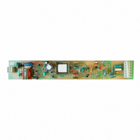
Specifications of STEVAL-ILB001V2
STEVAL-ILB001V2
Available stocks


Related parts for STEVAL-ILB001V2


STEVAL-ILB001V2 Summary of contents
Page 1
Simple cost-effective PFC using Bipolar Transistors Introduction This note deals with the implementation of a Power Factor Correction (PFC Discontinuous-mode Boost Converter where a PFC stage is achieved with a power bipolar transistor driven in self oscillating configuration. ...
Page 2
Contents Contents 1 PFC solutions for low-medium power HF Ballasts . . . . . . . . . . . . . . . . 5 1.1 Application description . . . . . . . . . . ...
Page 3
AN2349 List of tables Table 1. 40W Demoboard 220V bill of materials . . . . . . . . . . . . . . . . . . . . . . . . . . . . ...
Page 4
List of figures List of figures Figure 1. Valley Fill circuit schematic diagram . . . . . . . . . . . . . . . . . . . . . . . . . . . ...
Page 5
AN2349 1 PFC solutions for low-medium power HF Ballasts The Valley Fill circuit is an example of a low-cost passive PFC available on the market. Figure 1. Valley Fill circuit schematic diagram Figure 2. Valley Fll input current waveform The ...
Page 6
PFC solutions for low-medium power HF Ballasts Figure 3. Active PFC with IC and MOSFET in boost topology The proposed Bipolar PFC solution targets the low-cost HF Ballast market provides a simple cost-effective solution ...
Page 7
AN2349 control the PFC stage and reduces the Imain distortion achieving a THD in the range of about 30%, with a shape of the current drawn from the main as shown in Figure 5. Ts modulation in bipolar PFC Figure ...
Page 8
PFC solutions for low-medium power HF Ballasts Figure 7. Detail of storage time value and istant The PWM signal acts on T transformer normally used in the ballast. 8/30 Figure 8. Injected ...
Page 9
AN2349 2 Feedback block The duty cycle modulation performed by the Basic Solution shown in effective to achieve high THD values and no protection task can be implemented against overoload or high VAC values. A negative feedback network has been ...
Page 10
Feedback block The network thanks to a smart combination of three input signals. 1. Input 1 comes from the Main Voltage and it'is used to limit the amount of the distortion improving the THD. 2. Input ...
Page 11
AN2349 The overall storage time modulation achieved by the Bipolar PFC working with the negative feedback network is evident in detected on the oscilloscope at t Figure 14. Detail of Storage time value in t Injected charges Injected charges Storage ...
Page 12
Selection of boost output inductor L1 3 Selection of boost output inductor L The boost output inductor L instantaneous input power in order to obtain the minimum I discontinuous mode operation. This calculation is made considering a working operation at ...
Page 13
AN2349 Equation ------------- - = f SW where according to the working operation, LI contains the sinusoidal modulation of the main current with 30°<ωt<150°. In order to calculate I Equation 8 but I is also ...
Page 14
Selection of boost output inductor L1 Figure 17. Current on the electrolytic capacitor Thus for 0<ωt<Π: Equation 12 , the continuous component, is the mean value of ...
Page 15
AN2349 where from Equation the electrolytic capacitor, while X electrolytic capacitor, with f Equalizing Equation 16 Equation 18 and resolving by C: Equation where PP RIPPLE 2 I =2*P 17, the I -2I /π ...
Page 16
PFC driving network 4 PFC driving network The network composed by the capacitor and resistor in series to the base of the power bipolar transistor T1 are chosen in order to fix the duty-cycle at level less than 50% in ...
Page 17
AN2349 3. End collector current with di/dt < 0 Figure 20. Inductor current with di/dt<0 and transformer voltage shape The first condition is considered for our reference design, di/dt > 0, and in particular the slope on the point A ...
Page 18
PFC driving network The output voltage V Equation 20 V 2.5V = where C 0 the T BE voltage. 1 The shape of the transformer voltage in a half period T/2 is: Equation 21 After the initial instant, the capacitor ...
Page 19
AN2349 Figure 22. Collector current and base current shape Since v (t )=Q/C= Equation 25 where it has been imposed Ib Now from Equation 20 Equation 26 where V =1V is the base-emitter voltage of the device at ...
Page 20
PFC driving network You consider the instant of the main sinusoidal in which the collector current I reaches its maximum value and the base current Ib without modulation yet (see Multiplying this value for T/2, the amount of charge on ...
Page 21
AN2349 Equation 34 Now, the amount of charge on the collector of T2 is: Equation 35 with Equation 36 Now the I at the instant where the main voltage reaches its max value, v(t)=V Bmin We consider Equation 37 Equation ...
Page 22
PFC driving network Equation 43 From Equation 36, we can obtain Equation 44 Then the amount of charge on the T Equation 45 So, the total amount of charge on the capacitor C Equation 46 Substituting Equation 46 Equation 47 ...
Page 23
AN2349 5 T Transformer and L 5.1 220V design The transformer T has to be choosen as following: 1. The core type is N87-EFD25/13/9 by Epcos 2. The wire gauge used to wind the transformer is 0. The ...
Page 24
T Transformer and L1 inductor specifications Figure 24. 40W demoboard electrical schematic 24/30 AN2349 ...
Page 25
AN2349 Figure 25. 40W demoboard PCB layout and mounting components Table 1. 40W Demoboard 220V bill of materials Item Qty 1 5 D1… D17,D7, D9,D10,D11 BA159 4 2 D8, D13 T Transformer and L1 inductor ...
Page 26
T Transformer and L1 inductor specifications Table 1. 40W Demoboard 220V bill of materials (continued) Item Qty 5 1 Dz2 Dz1 ...
Page 27
AN2349 Table 1. 40W Demoboard 220V bill of materials (continued) Item Qty D14 Table 2. 40W Demoboard 120V bill of materials Item Qty 1 5 D1… D7,D9,D10,D11,D14 BA159 4 2 ...
Page 28
T Transformer and L1 inductor specifications Table 2. 40W Demoboard 120V bill of materials (continued) Item Qty R10 31 1 R11 32 1 R12 33 1 R13 34 1 ...
Page 29
AN2349 6 Revision history Table 3. Document revision history Date 06-Jun-2006 Revision 1 Initial release Revision history Changes 29/30 ...
Page 30
... Information in this document is provided solely in connection with ST products. STMicroelectronics NV and its subsidiaries (“ST”) reserve the right to make changes, corrections, modifications or improvements, to this document, and the products and services described herein at any time, without notice. All ST products are sold pursuant to ST’s terms and conditions of sale. ...