LMK03200EVAL National Semiconductor, LMK03200EVAL Datasheet - Page 38
LMK03200EVAL
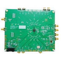
Manufacturer Part Number
LMK03200EVAL
Description
BOARD EVALUATION LMK03200
Manufacturer
National Semiconductor
Specifications of LMK03200EVAL
Main Purpose
Timing, Clock Conditioner
Embedded
No
Utilized Ic / Part
LMK03200
Primary Attributes
3 LVDS & 5 LVPECL Outputs, Integrated PLL & VCO
Secondary Attributes
3.15 V ~ 3.45 V Supply
Silicon Manufacturer
National
Silicon Core Number
LMK03200
Kit Application Type
Clock & Timing
Application Sub Type
Precision Clock Conditioner
Kit Contents
Board, Cable
Lead Free Status / RoHS Status
Lead free / RoHS Compliant


www.national.com
3.10 DIFFERENTIAL VOLTAGE MEASUREMENT
TERMINOLOGY
The differential voltage of a differential signal can be de-
scribed by two different definitions causing confusion when
reading datasheets or communicating with other engineers.
This section will address the measurement and description of
a differential signal so that the reader will be able to under-
stand and discern between the two different definitions when
used.
The first definition used to describe a differential signal is the
absolute value of the voltage potential between the inverting
and non-inverting signal. The symbol for this first measure-
ment is typically V
voltage is being described.
The second definition used to describe a differential signal is
to measure the potential of the non-inverting signal with re-
spect to the inverting signal. The symbol for this second
measurement is V
in the IC does this signal exist with respect to ground, it only
exists in reference to its differential pair. V
directly by oscilloscopes with floating references, otherwise
this value can be calculated as twice the value of V
scribed in the first description.
Figure 19
side-by-side for inputs and outputs respectively. The V
V
verting and inverting signals toggle between with respect to
ground. V
verting signal is considered the reference, the non-inverting
signal voltage potential is now increasing and decreasing
above and below the non-inverting reference. Thus the peak-
to-peak voltage of the differential signal can be measured.
Hence V
often defined as volts peak-to-peak (V
OD
definitions show V
ID
and
SS
and V
input and output definitions show that if the in-
Figure 20
OD
ID
SS
or V
are often defined as volts (V) and V
and is a calculated parameter. Nowhere
A
OD
illustrate the two different definitions
and V
depending on if an input or output
B
DC levels that the non-in-
PP
).
SS
can be measured
OD
as de-
ID
SS
and
is
38
Refer to application note AN-912 Common Data Transmis-
sion Parameters and their Definitions for more information.
FIGURE 19. Two Different Definitions for Differential
FIGURE 20. Two Different Definitions for Differential
Output Signals
Input Signals
30088775
30088774
Related parts for LMK03200EVAL
Image
Part Number
Description
Manufacturer
Datasheet
Request
R

Part Number:
Description:
Precision 0-delay Clock Conditioner With Integrated Vco
Manufacturer:
National Semiconductor Corporation
Datasheet:

Part Number:
Description:
National Semiconductor [8-Bit D/A Converter]
Manufacturer:
National Semiconductor
Datasheet:
Part Number:
Description:
National Semiconductor [Media Coprocessor]
Manufacturer:
National Semiconductor
Datasheet:
Part Number:
Description:
Digitally Controlled Tone and Volume Circuit with Stereo Audio Power Amplifier, Microphone Preamp Stage and National 3D Sound
Manufacturer:
National Semiconductor
Datasheet:
Part Number:
Description:
Digitally Controlled Tone and Volume Circuit with Stereo Audio Power Amplifier, Microphone Preamp Stage and National 3D Sound
Manufacturer:
National Semiconductor
Datasheet:
Part Number:
Description:
AC97 Rev 2 Codec with Sample Rate Conversion and National 3D Sound
Manufacturer:
National Semiconductor
Part Number:
Description:
Manufacturer:
National Semiconductor
Datasheet:
Part Number:
Description:
Manufacturer:
National Semiconductor
Datasheet:
Part Number:
Description:
General Purpose, Low Voltage, Low Power, Rail-to-Rail Output Operational Amplifiers
Manufacturer:
National Semiconductor
Datasheet:
Part Number:
Description:
8-bit 20 MSPS flash A/D converter.
Manufacturer:
National Semiconductor
Datasheet:
Part Number:
Description:
Low Noise Quad Operational Amplifier
Manufacturer:
National Semiconductor
Datasheet:
Part Number:
Description:
Quad Differential Line Receivers
Manufacturer:
National Semiconductor
Datasheet:
Part Number:
Description:
Quad High Speed Trapezoidal? Bus Transceiver
Manufacturer:
National Semiconductor
Datasheet:
Part Number:
Description:
Dual Line Receiver
Manufacturer:
National Semiconductor
Datasheet: