LMK03200EVAL National Semiconductor, LMK03200EVAL Datasheet - Page 8
LMK03200EVAL
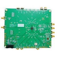
Manufacturer Part Number
LMK03200EVAL
Description
BOARD EVALUATION LMK03200
Manufacturer
National Semiconductor
Specifications of LMK03200EVAL
Main Purpose
Timing, Clock Conditioner
Embedded
No
Utilized Ic / Part
LMK03200
Primary Attributes
3 LVDS & 5 LVPECL Outputs, Integrated PLL & VCO
Secondary Attributes
3.15 V ~ 3.45 V Supply
Silicon Manufacturer
National
Silicon Core Number
LMK03200
Kit Application Type
Clock & Timing
Application Sub Type
Precision Clock Conditioner
Kit Contents
Board, Cable
Lead Free Status / RoHS Status
Lead free / RoHS Compliant


www.national.com
I
I
f
V
V
SLEW
f
V
V
SLEW
f
I
I
I
I
I
I
CC
CC
OSCin
FBCLKin
PD
SRCE
SINK
CPout
CPout
CPout
CPout
ID
OSCin
ID
FBCLKin
Electrical Characteristics
(3.15 V
most likely parametric norms at Vcc = 3.3 V, T
characterization and are not guaranteed).
Symbol
PD
OSCin
FBCLKin
CPout
CPout
TRI
%MIS
VTUNE
TEMP
OSCin
FBCLKin
≤
Vcc
Power Supply Current
(Note 5)
Power Down Current
Reference Oscillator Input Frequency
Range
Reference Oscillator Differential Input
Voltage
Reference Oscillator Single-ended Input
Voltage
Reference Oscillator Input Slew Rate
13)
External Feedback Clock Input Frequency
Range
External Feedback Clock Differential Input
Voltage
External Feedback Clock Single-ended
Input Voltage
External Feedback Clock Input Slew Rate
(Note 13)
Phase Detector Frequency
Charge Pump Source Current
Charge Pump Sink Current
Charge Pump TRI-STATE
Magnitude of Charge Pump
Sink vs. Source Current Mismatch
Magnitude of Charge Pump
Current vs. Charge Pump Voltage
Variation
Magnitude of Charge Pump Current vs.
Temperature Variation
≤
3.45 V, -40 °C
(Notes 6, 13)
(Note 13)
(Notes 6, 13)
(Note 13)
Parameter
≤
T
A
≤
85 °C, Differential Inputs/Outputs; Vboost=0; except as specified. Typical values represent
®
Current
(Note 4)
A
External Feedback Clock Input
= 25 °C, and at the Recommended Operation Conditions at the time of product
(Note
Reference Oscillator Input
Current Consumption
Entire device; one LVDS and one
LVPECL clock enabled; no divide; no
delay.
Entire device; All Outputs Off (no
emitter resistors placed)
POWERDOWN = 1
AC coupled
AC coupled; Unused pin AC coupled to
GND
20% to 80%; For each input pin
AC coupled
AC coupled; Unused pin AC coupled to
GND
20% to 80%; For each input pin
V
V
V
V
V
V
V
V
0.5 V < V
V
T
0.5 V < V
T
A
A
CPout
CPout
CPout
CPout
CPout
CPout
CPout
CPout
CPout
= 25°C
= 25°C
PLL
= Vcc/2, PLL_CP_GAIN = 1x
= Vcc/2, PLL_CP_GAIN = 4x
= Vcc/2, PLL_CP_GAIN = 16x
= Vcc/2, PLL_CP_GAIN = 32x
= Vcc/2, PLL_CP_GAIN = 1x
= Vcc/2, PLL_CP_GAIN = 4x
= Vcc/2, PLL_CP_GAIN = 16x
= Vcc/2, PLL_CP_GAIN = 32x
= Vcc / 2
8
CPout
CPout
Conditions
< Vcc - 0.5 V
< Vcc - 0.5 V
0.15
0.15
Min
0.2
0.2
0.2
0.2
1
1
-1600
-3200
161.8
1600
3200
-100
-400
Typ
100
400
0.5
0.5
86
5
2
3
4
4
Max
200
800
1.6
2.0
1.6
2.0
40
10
Units
MHz
MHz
MHz
V/ns
V/ns
Vpp
Vpp
mA
mA
µA
μA
nA
%
%
%
V
V
Related parts for LMK03200EVAL
Image
Part Number
Description
Manufacturer
Datasheet
Request
R

Part Number:
Description:
Precision 0-delay Clock Conditioner With Integrated Vco
Manufacturer:
National Semiconductor Corporation
Datasheet:

Part Number:
Description:
National Semiconductor [8-Bit D/A Converter]
Manufacturer:
National Semiconductor
Datasheet:
Part Number:
Description:
National Semiconductor [Media Coprocessor]
Manufacturer:
National Semiconductor
Datasheet:
Part Number:
Description:
Digitally Controlled Tone and Volume Circuit with Stereo Audio Power Amplifier, Microphone Preamp Stage and National 3D Sound
Manufacturer:
National Semiconductor
Datasheet:
Part Number:
Description:
Digitally Controlled Tone and Volume Circuit with Stereo Audio Power Amplifier, Microphone Preamp Stage and National 3D Sound
Manufacturer:
National Semiconductor
Datasheet:
Part Number:
Description:
AC97 Rev 2 Codec with Sample Rate Conversion and National 3D Sound
Manufacturer:
National Semiconductor
Part Number:
Description:
Manufacturer:
National Semiconductor
Datasheet:
Part Number:
Description:
Manufacturer:
National Semiconductor
Datasheet:
Part Number:
Description:
General Purpose, Low Voltage, Low Power, Rail-to-Rail Output Operational Amplifiers
Manufacturer:
National Semiconductor
Datasheet:
Part Number:
Description:
8-bit 20 MSPS flash A/D converter.
Manufacturer:
National Semiconductor
Datasheet:
Part Number:
Description:
Low Noise Quad Operational Amplifier
Manufacturer:
National Semiconductor
Datasheet:
Part Number:
Description:
Quad Differential Line Receivers
Manufacturer:
National Semiconductor
Datasheet:
Part Number:
Description:
Quad High Speed Trapezoidal? Bus Transceiver
Manufacturer:
National Semiconductor
Datasheet:
Part Number:
Description:
Dual Line Receiver
Manufacturer:
National Semiconductor
Datasheet: