KDC5514-Q48EVAL Intersil, KDC5514-Q48EVAL Datasheet - Page 24
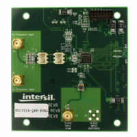
KDC5514-Q48EVAL
Manufacturer Part Number
KDC5514-Q48EVAL
Description
DAUGHTER CARD FOR KAD5514
Manufacturer
Intersil
Series
FemtoCharge™r
Datasheets
1.KAD5514P-25Q72.pdf
(34 pages)
2.KMB-001LEVALZ.pdf
(7 pages)
3.KDC5514EVALZ.pdf
(9 pages)
Specifications of KDC5514-Q48EVAL
Number Of Adc's
1
Number Of Bits
14
Sampling Rate (per Second)
250M
Data Interface
Parallel
Inputs Per Adc
1 Differential
Input Range
1.47 Vpp
Power (typ) @ Conditions
429mW @ 250MSPS
Voltage Supply Source
Single Supply
Operating Temperature
-40°C ~ 85°C
Utilized Ic / Part
KAD5514P-25, KMB001 Motherboard
For Use With
KMB001LEVAL - MOTHERBOARD FOR LVDS ADC CARD
Lead Free Status / RoHS Status
Lead free / RoHS Compliant


Figures 38 and 39 illustrate the timing relationships for
2-byte and N-byte transfers, respectively. The operation for a
3-byte transfer can be inferred from these diagrams.
SPI Configuration
ADDRESS 0X00: CHIP_PORT_CONFIG
Bit ordering and SPI reset are controlled by this register. Bit
order can be selected as MSB to LSB (MSB first) or LSB to
MSB (LSB first) to accommodate various microcontrollers.
Bit 7 SDO Active
Bit 6 LSB First
Bit 5 Soft Reset
Bit 4 Reserved
Bits 3:0 These bits should always mirror bits 4:7 to avoid
ambiguity in bit ordering.
ADDRESS 0X02: BURST_END
If a series of sequential registers are to be set, burst mode
can improve throughput by eliminating redundant
addressing. In three-wire SPI mode the burst is ended by
pulling the CSB pin high. If the device is operated in two-wire
mode the CSB pin is not available. In that case, setting the
burst_end address determines the end of the transfer.
During a write operation, the user must be cautious to
transmit the correct number of bytes based on the starting
and ending addresses.
Setting this bit high configures the SPI to interpret serial
data as arriving in LSB to MSB order.
Setting this bit high resets all SPI registers to default values.
This bit should always be set high.
SCLK
SDIO
SCLK
SDIO
CSB
CSB
INSTRUCTION/ADDRESS
INSTRUCTION/ADDRESS
24
FIGURE 40. N-BYTE TRANSFER
FIGURE 39. 2-BYTE TRANSFER
KAD5514P
CSB STALLING
DATA WORD 1
CSB STALLING
LAST LEGAL
DATA WORD 1
Bits 7:0 Burst End Address
Device Information
ADDRESS 0X08: CHIP_ID
ADDRESS 0X09: CHIP_VERSION
The generic die identifier and a revision number,
respectively, can be read from these two registers.
Indexed Device Configuration/Control
ADDRESS 0X10: DEVICE_INDEX_A
A common SPI map, which can accommodate
single-channel or multi-channel devices, is used for all
Intersil ADC products. Certain configuration commands
(identified as Indexed in the SPI map) can be executed on a
per-converter basis. This register determines which
converter is being addressed for an Indexed command. It is
important to note that only a single converter can be
addressed at a time.
This register defaults to 00h, indicating that no ADC is
addressed. Error code ‘AD’ is returned if any indexed
register is read from without properly setting
device_index_A.
ADDRESS 0X20: OFFSET_COARSE
ADDRESS 0X21: OFFSET_FINE
The input offset of each ADC core can be adjusted in fine
and coarse steps. Both adjustments are made via an 8-bit
word as detailed in Table 7.
This register value determines the ending address of the
burst data.
DATA WORD N
DATA WORD 2
September 10, 2009
FN6804.2
Related parts for KDC5514-Q48EVAL
Image
Part Number
Description
Manufacturer
Datasheet
Request
R

Part Number:
Description:
Intersil Corporation [CMOS Serial Controller Interface]
Manufacturer:
Intersil Corporation
Datasheet:
Part Number:
Description:
Manufacturer:
Intersil Corporation
Datasheet:
Part Number:
Description:
357-036-542-201 CARDEDGE 36POS DL .156 BLK LOPRO
Manufacturer:
Intersil Corporation
Datasheet:
Part Number:
Description:
1024-Word x 4-Bit LSI Static RAM
Manufacturer:
Intersil Corporation
Datasheet:
Part Number:
Description:
General Purpose NPN Transistor Arrays FN341.4
Manufacturer:
Intersil Corporation
Datasheet:
Part Number:
Description:
CMOS 16-Bit Microprocessor
Manufacturer:
Intersil Corporation
Datasheet:
Part Number:
Description:
Manufacturer:
Intersil Corporation
Datasheet:
Part Number:
Description:
Manufacturer:
Intersil Corporation
Datasheet:
Part Number:
Description:
Manufacturer:
Intersil Corporation
Datasheet:
Part Number:
Description:
Manufacturer:
Intersil Corporation
Datasheet:
Part Number:
Description:
CMOS 6-Bit Latch and Decoder Memory Interfaces
Manufacturer:
Intersil Corporation
Datasheet:
Part Number:
Description:
CA3046General Purpose NPN Transistor Arrays
Manufacturer:
Intersil Corporation
Datasheet:
Part Number:
Description:
Manufacturer:
Intersil Corporation
Datasheet:
Part Number:
Description:
TR909 DLC/FLC SLIC with Low Power Standby
Manufacturer:
Intersil Corporation
Datasheet:
Part Number:
Description:
Manufacturer:
Intersil Corporation
Datasheet: