KDC5514-Q48EVAL Intersil, KDC5514-Q48EVAL Datasheet - Page 30
KDC5514-Q48EVAL
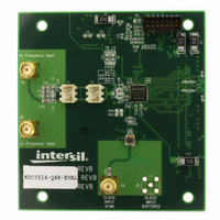
Manufacturer Part Number
KDC5514-Q48EVAL
Description
DAUGHTER CARD FOR KAD5514
Manufacturer
Intersil
Series
FemtoCharge™r
Datasheets
1.KAD5514P-25Q72.pdf
(34 pages)
2.KMB-001LEVALZ.pdf
(7 pages)
3.KDC5514EVALZ.pdf
(9 pages)
Specifications of KDC5514-Q48EVAL
Number Of Adc's
1
Number Of Bits
14
Sampling Rate (per Second)
250M
Data Interface
Parallel
Inputs Per Adc
1 Differential
Input Range
1.47 Vpp
Power (typ) @ Conditions
429mW @ 250MSPS
Voltage Supply Source
Single Supply
Operating Temperature
-40°C ~ 85°C
Utilized Ic / Part
KAD5514P-25, KMB001 Motherboard
For Use With
KMB001LEVAL - MOTHERBOARD FOR LVDS ADC CARD
Lead Free Status / RoHS Status
Lead free / RoHS Compliant


Equivalent Circuits
72 Pin/48 Pin Package Options
The KAD5514 is available in both 72 pin and 48 pin
packages. The 48 pin package option supports LVDS DDR
only. A reduced set of pin selectable functions are available
in the 48 pin package due to the reduced pinout;
(OUTMODE, OUTFMT, and CLKDIV pins are not available).
Table 17 shows the default state for these functions for the
48 pin package. Note that these functions are available
through the SPI, allowing a user to set these modes as they
desire, offering the same flexibility as the 72 pin package
option. DC and AC performance of the ADC is equivalent for
both package options.
.
ADC Evaluation Platform
Intersil offers an ADC Evaluation platform which can be used
to evaluate any of the KADxxxxx ADC family. The platform
consists of a FPGA based data capture motherboard and a
family of ADC daughtercards. This USB based platform
allows a user to quickly evaluate the ADC’s performance at a
user’s specific application frequency requirements. More
information is available at
http://www.intersil.com/converters/adc_eval_platform/
Layout Considerations
Split Ground and Power Planes
Data converters operating at high sampling frequencies
require extra care in PC board layout. Many complex board
designs benefit from isolating the analog and digital
sections. Analog supply and ground planes should be laid
out under signal and clock inputs. Locate the digital planes
FUNCTION
OUTMODE
OUTFMT
CLKDIV
TABLE 17. 48 PIN SPI - ADDRESSABLE FUNCTIONS
DESCRIPTION
Clock Divider
Output Driver
Data Coding
Mode
(Continued)
30
0.535V
Two’s Complement
LVDS, 3mA (DDR)
DEFAULT STATE
Divide by 1
+
–
FIGURE 49. VCM_OUT OUTPUT
KAD5514P
under outputs and logic pins. Grounds should be joined
under the chip.
Clock Input Considerations
Use matched transmission lines to the transformer inputs for
the analog input and clock signals. Locate transformers and
terminations as close to the chip as possible.
Exposed Paddle
The exposed paddle must be electrically connected to
analog ground (AVSS) and should be connected to a large
copper plane using numerous vias for optimal thermal
performance.
Bypass and Filtering
Bulk capacitors should have low equivalent series
resistance. Tantalum is a good choice. For best
performance, keep ceramic bypass capacitors very close to
device pins. Longer traces will increase inductance, resulting
in diminished dynamic performance and accuracy. Make
sure that connections to ground are direct and low
impedance. Avoid forming ground loops.
LVDS Outputs
Output traces and connections must be designed for 50Ω
(100Ω differential) characteristic impedance. Keep traces
direct and minimize bends where possible. Avoid crossing
ground and power-plane breaks with signal traces.
LVCMOS Outputs
Output traces and connections must be designed for 50Ω
characteristic impedance.
Unused Inputs
Standard logic inputs (RESETN, CSB, SCLK, SDIO, SDO)
which will not be operated do not require connection to
ensure optimal ADC performance. These inputs can be left
floating if they are not used. Tri-level inputs (NAPSLP,
OUTMODE, OUTFMT, CLKDIV) accept a floating input as a
valid state, and therefore should be biased according to the
desired functionality.
AVDD
VCM
September 10, 2009
FN6804.2
Related parts for KDC5514-Q48EVAL
Image
Part Number
Description
Manufacturer
Datasheet
Request
R

Part Number:
Description:
Intersil Corporation [CMOS Serial Controller Interface]
Manufacturer:
Intersil Corporation
Datasheet:
Part Number:
Description:
Manufacturer:
Intersil Corporation
Datasheet:
Part Number:
Description:
357-036-542-201 CARDEDGE 36POS DL .156 BLK LOPRO
Manufacturer:
Intersil Corporation
Datasheet:
Part Number:
Description:
1024-Word x 4-Bit LSI Static RAM
Manufacturer:
Intersil Corporation
Datasheet:
Part Number:
Description:
General Purpose NPN Transistor Arrays FN341.4
Manufacturer:
Intersil Corporation
Datasheet:
Part Number:
Description:
CMOS 16-Bit Microprocessor
Manufacturer:
Intersil Corporation
Datasheet:
Part Number:
Description:
Manufacturer:
Intersil Corporation
Datasheet:
Part Number:
Description:
Manufacturer:
Intersil Corporation
Datasheet:
Part Number:
Description:
Manufacturer:
Intersil Corporation
Datasheet:
Part Number:
Description:
Manufacturer:
Intersil Corporation
Datasheet:
Part Number:
Description:
CMOS 6-Bit Latch and Decoder Memory Interfaces
Manufacturer:
Intersil Corporation
Datasheet:
Part Number:
Description:
CA3046General Purpose NPN Transistor Arrays
Manufacturer:
Intersil Corporation
Datasheet:
Part Number:
Description:
Manufacturer:
Intersil Corporation
Datasheet:
Part Number:
Description:
TR909 DLC/FLC SLIC with Low Power Standby
Manufacturer:
Intersil Corporation
Datasheet:
Part Number:
Description:
Manufacturer:
Intersil Corporation
Datasheet: