KDC5514-Q48EVAL Intersil, KDC5514-Q48EVAL Datasheet

DAUGHTER CARD FOR KAD5514

KDC5514-Q48EVAL

Manufacturer Part Number
KDC5514-Q48EVAL
Description
DAUGHTER CARD FOR KAD5514
Manufacturer
Intersil
Series
FemtoCharge™r

Specifications of KDC5514-Q48EVAL

Number Of Adc's
1
Number Of Bits
14
Sampling Rate (per Second)
250M
Data Interface
Parallel
Inputs Per Adc
1 Differential
Input Range
1.47 Vpp
Power (typ) @ Conditions
429mW @ 250MSPS
Voltage Supply Source
Single Supply
Operating Temperature
-40°C ~ 85°C
Utilized Ic / Part
KAD5514P-25, KMB001 Motherboard
For Use With
KMB001LEVAL - MOTHERBOARD FOR LVDS ADC CARD
Lead Free Status / RoHS Status
Lead free / RoHS Compliant
Konverter Analyzer User’s Guide
High-Speed ADC Evaluation
Platform
• Complete High-Speed ADC Measurement Solution
• 40MSPS to 500MSPS Operation
• Calculation of Critical ADC Parameters (SNR, SINAD,
• Multiple Display Modes: FFT, Time Domain, Logic
• Integrated SPI Control for ADC Configuration
• 18Mb (1MWord) Capture Depth
• Compatible with all Intersil High-Speed ADC
Evaluation Platform Overview
Intersil’s high-speed ADC evaluation platform consists of
custom designed hardware and software. The function of
the hardware is to provide power to the ADC and to
excite and/or measure the appropriate analog and digital
inputs and outputs. The software is required to configure
the device for initial operation, to modify the device
functionality or parameters, and to process and display
the output data.
Two versions of the software are provided to support two
different ADC families: version 1.15.6c supports all
KAD27XX and KAD5XXX devices, while version 1.20c
supports the ISLA11XP50 family. Refer to the Konverter
Installation Guide (AN1434) for details on installing and
running the different versions.
October 1, 2010
AN1433.4
SFDR, Harmonics, INL, DNL, Power)
Daughter Cards
Reference
10MHz
OUT
REF
REF
IN
Analog Input
RF Generator
RF Generator
(40-500MHz)
Low-Jitter
Low-Jitter
Clock
1
FIGURE 1. EVALUATION PLATFORM BLOCK DIAGRAM
MATLAB is a trademark of The MathWorks, Inc. Copyright Intersil Americas Inc. 2008-2010. All Rights Reserved
1-888-INTERSIL or 1-888-468-3774
CAUTION: These devices are sensitive to electrostatic discharge; follow proper IC Handling Procedures.
Analog Inputs
Application Note 1433
Attenuator
Optional
Hardware
There are two components in the hardware portion of the
evaluation platform: the daughter card and the
motherboard (Figure 1). The ADC is contained on the
daughter card, which routes power from the
motherboard and contains the analog input circuitry,
clock drive and decoupling. The daughter card interfaces
to the motherboard through a mezzanine connector. The
motherboard contains a USB interface, an FPGA and
SRAM. The motherboard serves as the interface between
the host PC and the ADC daughter card. Most of the ADC
functionality is controlled by the motherboard, although
some daughter cards have jumpers to set certain
operating modes. The FPGA accepts output data from the
ADC and buffers it in the SRAMs before passing it to the
PC at a lower speed for post-processing. The maximum
buffer depth is approximately one million words.
The user must supply low-jitter RF generators for the
clock and analog inputs. Recommendations of suitable
generators can be found in Appendix A.
Many low-jitter RF generators exhibit high harmonic
spectral content relative to the ADC performance. A
band-pass filter is recommended to attenuate the
harmonics. A wideband attenuator in series with the
band-pass filter is also recommended for daughter cards
without on-board attenuators. Current spikes from the
ADC’s switched capacitor sample-and-hold amplifier can
create signal reflections in the coaxial cable. The
attenuator reduces these reflections and improves
performance.
All other trademarks mentioned are the property of their respective owners.
|
Intersil (and design) is a registered trademark of Intersil Americas Inc.
Clock Inputs
Daughter
Mezzanine
Connector
Card
ADC
Motherboard
FPGA
KMB001
SRAM
SRAM
USB
+5V
To Host PC
USB

Related parts for KDC5514-Q48EVAL

KDC5514-Q48EVAL Summary of contents

Page 1

... CAUTION: These devices are sensitive to electrostatic discharge; follow proper IC Handling Procedures. | 1-888-INTERSIL or 1-888-468-3774 Intersil (and design registered trademark of Intersil Americas Inc. MATLAB is a trademark of The MathWorks, Inc. Copyright Intersil Americas Inc. 2008-2010. All Rights Reserved All other trademarks mentioned are the property of their respective owners. USB To Host PC ...

Page 2

Software The software component is Konverter Analyzer, a graphical user interface (GUI) created with MATLAB™. A MATLAB Component Runtime engine is supplied, which executes a compiled version of the m-files. Therefore a stand-alone version of MATLAB is not required to ...

Page 3

... OS occurs at the unit ADC sample rate. When the ISLA112P50 daughter card is connected, the Background Interleave Cal button is enabled. This allows the user to turn the Intersil Interleave Engine (I2E off. Full control of the I2E block is accomplished using the Interleave Control Panel. Logic Display ...

Page 4

Menus File The file menu allows the user to load or save a data record or configuration file as well as print the current display. Data is stored as an ASCII file in comma- separated value (CSV) format. Configuration files ...

Page 5

The FFT dialog (Figure 7) allows the selection of several parameters that impact the FFT display and parametric calculations. • Samples: The length of the data record • Sample Rate: The ADC sample rate. This option is unavailable unless the ...

Page 6

The Register Control Panel (Figure 9) is used to adjust the gain, offset and clock skew of the ADC cores and control various functional settings such as data format and output mode. The Phase setting is differential in nature and ...

Page 7

... Contact Intersil Technical Support for recommendations. Appendix B: Daughter Cards KDC5512EVALZ, KDC5512HEVALZ, KDC5512-50EVALZ, KDC5514EVALZ, ISLA112P50IR72EV1Z These daughter cards use a common design to accommodate the single-input devices from the KAD55XX and ISLA11XP50 families. They allow for two clock input paths and two analog input paths ...

Page 8

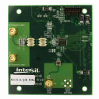
... Frequency path, remove 0Ω resistors R16 and R17 and install 0Ω resistors R18 and R20. KDC5512-Q48EVAL, KDC5512H-Q48EVAL, KDC5514-Q48EVAL These daughter cards contain the 48-QFN version of the product. To switch to the Lo Frequency path, remove 0Ω resistors R14 and R15 and install 0Ω resistors R16 and R18 ...

Page 9

... Intersil Corporation reserves the right to make changes in circuit design, software and/or specifications at any time without notice. Accordingly, the reader is cautioned to verify that the Application Note or Technical Brief is current before proceeding. For information regarding Intersil Corporation and its products, see www.intersil.com ...

Related keywords