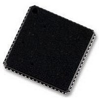
AD9248BCP-40EBZ Analog Devices Inc, AD9248BCP-40EBZ Datasheet - Page 10

AD9248BCP-40EBZ
Manufacturer Part Number
AD9248BCP-40EBZ
Description
BOARD EVAL WITH AD9248BCP-40
Manufacturer
Analog Devices Inc
Specifications of AD9248BCP-40EBZ
Number Of Adc's
2
Number Of Bits
14
Sampling Rate (per Second)
40M
Data Interface
Parallel
Inputs Per Adc
1 Differential
Input Range
2 Vpp
Power (typ) @ Conditions
360mW @ 40MSPS
Voltage Supply Source
Single
Operating Temperature
-40°C ~ 85°C
Utilized Ic / Part
AD9248BCP-40
Silicon Manufacturer
Analog Devices
Application Sub Type
ADC
Kit Application Type
Data Converter
Silicon Core Number
AD9248
Kit Contents
Board
Power Dissipation Pd
400mW
Termination Type
SMD
Lead Free Status / RoHS Status
Lead free / RoHS Compliant
Lead Free Status / RoHS Status
Lead free / RoHS Compliant, Lead free / RoHS Compliant
AD9248
Table 6. 64-Lead LQFP and 64-Lead LFCSP Pin Function Descriptions
Pin No.
1, 4, 13, 16
2
3
5, 12, 17, 64
6
7
8
9
10
11
14
15
18
19
20
21
22
23 to 27,
30 to 38
28, 40, 53
29, 41, 52
39
42 to 51,
54 to 57
58
59
60
61
62
63
Mnemonic
AGND
VIN+_A
VIN−_A
AVDD
REFT_A
REFB_A
VREF
SENSE
REFB_B
REFT_B
VIN−_B
VIN+_B
CLK_B
DCS
DFS
PDWN_B
OEB_B
D0_B (LSB) to
D13_B (MSB)
DRGND
DRVDD
OTR_B
D0_A (LSB) to
D13_A (MSB)
OTR_A
OEB_A
PDWN_A
MUX_SELECT
SHARED_REF
CLK_A
EP
Description
Analog Ground.
Analog Input Pin (+) for Channel A.
Analog Input Pin (−) for Channel A.
Analog Power Supply.
Differential Reference (+) for Channel A.
Differential Reference (−) for Channel A.
Voltage Reference Input/Output.
Reference Mode Selection.
Differential Reference (−) for Channel B.
Differential Reference (+) for Channel B.
Analog Input Pin (−) for Channel B.
Analog Input Pin (+) for Channel B.
Clock Input Pin for Channel B.
Enable Duty Cycle Stabilizer (DCS) Mode.
Data Output Format Select Pin (Low for Offset Binary, High for Twos Complement).
Power-Down Function Selection for Channel B.
Logic 0 enables Channel B. Logic 1 powers down Channel B (outputs static, not High-Z).
Output Enable Pin for Channel B.
Logic 0 enables Data Bus B. Logic 1 sets outputs to High-Z.
Channel B Data Output Bits.
Digital Output Ground.
Digital Output Driver Supply. Must be decoupled to DRGND with a minimum 0.1 μF capacitor.
Recommended decoupling is 0.1 μF capacitor in parallel with 10 μF capacitor.
Out-of-Range Indicator for Channel B.
Channel A Data Output Bits.
Out-of-Range Indicator for Channel A.
Output Enable Pin for Channel A.
Logic 0 enables Data Bus A. Logic 1 sets outputs to High-Z.
Power-Down Function Selection for Channel A.
Logic 0 enables Channel A. Logic 1 powers down Channel A (outputs static, not High-Z).
Data Multiplexed Mode.
(See Data Format section for how to enable; high setting disables output data multiplexed mode.)
Shared Reference Control Pin (Low for Independent Reference Mode, High for Shared Reference Mode).
Clock Input Pin for Channel A.
For the 64-Lead LFCSP only, there is an exposed pad that must connect to AGND.
Rev. B | Page 10 of 48


