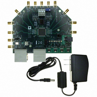
AD9272-65EBZ Analog Devices Inc, AD9272-65EBZ Datasheet - Page 24

AD9272-65EBZ
Manufacturer Part Number
AD9272-65EBZ
Description
BOARD EVAL AD9272
Manufacturer
Analog Devices Inc
Specifications of AD9272-65EBZ
Design Resources
Powering AD9272 with ADP5020 Switching Regulator PMU for Increased Efficiency (CN0135)
Number Of Adc's
8
Number Of Bits
12
Sampling Rate (per Second)
65M
Data Interface
Serial
Inputs Per Adc
1 Differential
Input Range
733 mVpp
Power (typ) @ Conditions
1.69W @ 65MSPS
Voltage Supply Source
Analog and Digital
Operating Temperature
-40°C ~ 85°C
Utilized Ic / Part
AD9272
Silicon Manufacturer
Analog Devices
Application Sub Type
ADC
Kit Application Type
Data Converter
Silicon Core Number
AD9272
Kit Contents
Board
Development Tool Type
Hardware - Eval/Demo Board
Rohs Compliant
Yes
Lead Free Status / RoHS Status
Lead free / RoHS Compliant
AD9272
LNA Noise
The short-circuit noise voltage (input-referred noise) is an impor-
tant limit on system performance. The short-circuit input-referred
noise voltage for the LNA is 0.85 nV/√Hz at a gain of 21.3 dB,
including the VGA noise at a VGA postamp gain of 27 dB. These
measurements, which were taken without a feedback resistor,
provide the basis for calculating the input noise and noise figure
(NF) performance of the configurations shown in Figure 40.
Figure 41 and Figure 42 are simulations of noise figure vs. R
results using these configurations and an input-referred noise
voltage of 3.8 nV/√Hz for the VGA. Unterminated (R
operation exhibits the lowest equivalent input noise and noise
figure. Figure 42 shows the noise figure vs. source resistance
rising at low R
with the source noise—and at high R
from R
The main purpose of input impedance matching is to improve the
transient response of the system. With resistive termination, the
input noise increases due to the thermal noise of the matching
resistor and the increased contribution of the input voltage
noise generator of the LNA. With active impedance matching,
however, the contributions of both are smaller (by a factor of
1/(1 + LNA Gain)) than they would be for resistive termination.
FB
. The lowest NF is achieved when R
S
LI-x
LI-x
LI-x
—where the LNA voltage noise is large compared
+
–
+
–
+
–
Figure 40. Input Configurations
ACTIVE IMPEDANCE MATCH
R
R
R
RESISTIVE TERMINATION
S
S
S
R
UNTERMINATED
IN
=
R
R
R
1 + A/2
IN
IN
IN
R
FB
R
S
S
R
due to the noise contribution
FB
V
V
V
S
OUT
OUT
OUT
matches R
FB
= ∞)
IN
.
S
Rev. C | Page 24 of 44
Figure 41 shows the relative noise figure performance. In this
graph, the input impedance was swept with R
match at each point. The noise figures for a source impedance of
50 Ω are 7.3 dB, 4.2 dB, and 2.8 dB for the resistive termination,
active termination, and unterminated configurations, respectively.
The noise figures for 200 Ω are 4.5 dB, 1.7 dB, and 1 dB,
respectively.
Figure 42 shows the noise figure as it relates to R
of R
Active Termination Matched, and Unterminated Inputs, V
IN
, which is helpful for design purposes.
12.0
10.5
9.0
7.5
6.0
4.5
3.0
1.5
Figure 42. Noise Figure vs. R
8
7
6
5
4
3
2
1
0
0
10
Figure 41. Noise Figure vs. R
10
UNTERMINATED
Active Termination Matched Inputs, V
R
R
R
R
UNTERMINATED
IN
IN
IN
IN
= 50Ω
= 75Ω
= 100Ω
= 200Ω
RESISTIVE TERMINATION
S
for Various Fixed Values of R
R
R
S
100
S
100
S
for Resistive Termination,
(Ω)
(Ω)
ACTIVE TERMINATION
GAIN
S
to preserve the
S
= 0.8 V
for various values
GAIN
= 0.8 V
IN
,
1k
1k


