AD9272-65EBZ Analog Devices Inc, AD9272-65EBZ Datasheet - Page 3
AD9272-65EBZ
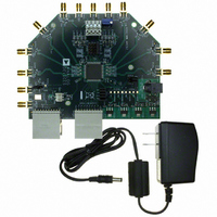
Manufacturer Part Number
AD9272-65EBZ
Description
BOARD EVAL AD9272
Manufacturer
Analog Devices Inc
Specifications of AD9272-65EBZ
Design Resources
Powering AD9272 with ADP5020 Switching Regulator PMU for Increased Efficiency (CN0135)
Number Of Adc's
8
Number Of Bits
12
Sampling Rate (per Second)
65M
Data Interface
Serial
Inputs Per Adc
1 Differential
Input Range
733 mVpp
Power (typ) @ Conditions
1.69W @ 65MSPS
Voltage Supply Source
Analog and Digital
Operating Temperature
-40°C ~ 85°C
Utilized Ic / Part
AD9272
Silicon Manufacturer
Analog Devices
Application Sub Type
ADC
Kit Application Type
Data Converter
Silicon Core Number
AD9272
Kit Contents
Board
Development Tool Type
Hardware - Eval/Demo Board
Rohs Compliant
Yes
Lead Free Status / RoHS Status
Lead free / RoHS Compliant


The AD9272 requires a LVPECL-/CMOS-/LVDS-compatible
sample rate clock for full performance operation. No external
reference or driver components are required for many
applications.
The ADC automatically multiplies the sample rate clock for
the appropriate LVDS serial data rate. A data clock (DCO±) for
capturing data on the output and a frame clock (FCO±) trigger
for signaling a new output byte are provided.
Powering down individual channels is supported to increase
battery life for portable applications. There is also a standby
mode option that allows quick power-up for power cycling. In
CW Doppler operation, the VGA, antialiasing filter (AAF), and
ADC are powered down. The power of the time gain control
(TGC) path scales with selectable speed grades.
The ADC contains several features designed to maximize flexibility
and minimize system cost, such as a programmable clock, data
alignment, and programmable digital test pattern generation. The
digital test patterns include built-in fixed patterns, built-in
pseudorandom patterns, and custom user-defined test patterns
entered via the serial port interface.
Rev. C | Page 3 of 44
Fabricated in an advanced CMOS process, the AD9272 is
available in a 16 mm × 16 mm, RoHS-compliant, 100-lead
TQFP. It is specified over the industrial temperature range of
−40°C to +85°C.
PRODUCT HIGHLIGHTS
1.
2.
3.
4.
5.
6.
Small Footprint. Eight channels are contained in a
small, space-saving package. A full TGC path, ADC, and
crosspoint switch are contained within a 100-lead, 16 mm ×
16 mm TQFP.
Low Power of 195 mW Per Channel at 40 MSPS.
Integrated Crosspoint Switch. This switch allows numerous
multichannel configuration options to enable the CW
Doppler mode.
Ease of Use. A data clock output (DCO±) operates up to
480 MHz and supports double data rate (DDR) operation.
User Flexibility. Serial port interface (SPI) control offers a wide
range of flexible features to meet specific system requirements.
Integrated Second-Order Antialiasing Filter. This filter is
placed between the VGA and the ADC and is programmable
from 8 MHz to 18 MHz.
AD9272
Related parts for AD9272-65EBZ
Image
Part Number
Description
Manufacturer
Datasheet
Request
R

Part Number:
Description:
±1.7g Dual-Axis IMEMS Accelerometer Evaluation Board
Manufacturer:
Analog Devices Inc
Datasheet:

Part Number:
Description:
Inertial Sensor Evaluation System
Manufacturer:
Analog Devices Inc
Datasheet:
Part Number:
Description:
Manufacturer:
Analog Devices Inc
Datasheet:
Part Number:
Description:
Manufacturer:
Analog Devices Inc
Datasheet:
Part Number:
Description:
Manufacturer:
Analog Devices Inc
Datasheet:
Part Number:
Description:
Manufacturer:
Analog Devices Inc
Datasheet:
Part Number:
Description:
Manufacturer:
Analog Devices Inc
Datasheet:
Part Number:
Description:
Manufacturer:
Analog Devices Inc
Datasheet:
Part Number:
Description:
Manufacturer:
Analog Devices Inc
Datasheet:
Part Number:
Description:
Manufacturer:
Analog Devices Inc
Datasheet:
Part Number:
Description:
Manufacturer:
Analog Devices Inc
Datasheet:
Part Number:
Description:
Manufacturer:
Analog Devices Inc
Datasheet:
Part Number:
Description:
Manufacturer:
Analog Devices Inc
Datasheet: