AD9272-65EBZ Analog Devices Inc, AD9272-65EBZ Datasheet - Page 42
AD9272-65EBZ
Manufacturer Part Number
AD9272-65EBZ
Description
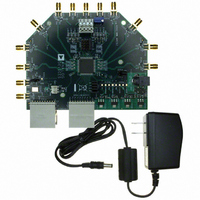
BOARD EVAL AD9272
Manufacturer
Analog Devices Inc
Specifications of AD9272-65EBZ
Design Resources
Powering AD9272 with ADP5020 Switching Regulator PMU for Increased Efficiency (CN0135)
Number Of Adc's
8
Number Of Bits
12
Sampling Rate (per Second)
65M
Data Interface
Serial
Inputs Per Adc
1 Differential
Input Range
733 mVpp
Power (typ) @ Conditions
1.69W @ 65MSPS
Voltage Supply Source
Analog and Digital
Operating Temperature
-40°C ~ 85°C
Utilized Ic / Part
AD9272
Silicon Manufacturer
Analog Devices
Application Sub Type
ADC
Kit Application Type
Data Converter
Silicon Core Number
AD9272
Kit Contents
Board
Development Tool Type
Hardware - Eval/Demo Board
Rohs Compliant
Yes
Lead Free Status / RoHS Status
Lead free / RoHS Compliant


AD9272
Addr.
(Hex)
0F
10
11
12
14
15
16
18
Register Name
Flex_channel_input
Flex_offset
Flex_gain
Bias_current
Output_mode
Output_adjust
Output_phase
Flex_vref
Bit 7
(MSB)
Filter cutoff frequency control
0000 = 1.3 × 1/3 × f
0001 = 1.2 × 1/3 × f
0010 = 1.1 × 1/3 × f
0011 = 1.0 × 1/3 × f
0100 = 0.9 × 1/3 × f
0101 = 0.8 × 1/3 × f
0110 = 0.7 × 1/3 × f
1000 = 1.3 × 1/4.5 × f
1001 = 1.2 × 1/4.5 × f
1010 = 1.1 × 1/4.5 × f
1011 = 1.0 × 1/4.5 × f
1100 = 0.9 × 1/4.5 × f
1101 = 0.8 × 1/4.5 × f
1110 = 0.7 × 1/4.5 × f
X
X
X
X
X
X
X
Bit 6
X
X
X
0 = LVDS
ANSI-644
(default)
1 = LVDS
low power,
(IEEE
1596.3
similar)
X
X
0 =
internal
reference
1 =
external
reference
SAMPLE
SAMPLE
SAMPLE
SAMPLE
SAMPLE
SAMPLE
SAMPLE
SAMPLE
SAMPLE
SAMPLE
SAMPLE
SAMPLE
SAMPLE
SAMPLE
(default)
Bit 5
6-bit LNA offset adjustment
10 0000 for LNA bias high, mid-high, mid-low (default)
10 0001 for LNA bias low
X
X
X
Output driver
termination
00 = none (default)
01 = 200 Ω
10 = 100 Ω
11 = 100 Ω
X
X
Rev. C | Page 42 of 44
Bit 4
X
X
X
X
X
Bit 3
X
PGA gain
00 = 21 dB
01 = 24 dB (default)
10 = 27 dB
11 = 30 dB
1
X
X
0011 = output clock phase adjust
(0000 through 1010)
(Default: 180° relative to data edge)
0000 = 0° relative to data edge
0001 = 60° relative to data edge
0010 = 120° relative to data edge
0011 = 180° relative to data edge
0100 = 240° relative to data edge
0101 = 300° relative to data edge
0110 = 360° relative to data edge
0111 = 420° relative to data edge
1000 = 480° relative to data edge
1001 = 540° relative to data edge
1010 = 600° relative to data edge
1011 to 1111 = 660° relative to data edge
X
Bit 2
X
X
Output
invert
1 = on
0 = off
(default)
X
X
Bit 1
X
LNA gain
00 = 15.6 dB
01 = 17.9 dB
10 = 21.3 dB
(default)
LNA bias
00 = high (default)
01 = mid-high
10 = mid-low
11 = low
00 = offset binary
(default)
01 = twos
complement
X
X
Bit 0
(LSB)
X
DCO±
and
FCO±
2× drive
strength
1 = on
0 = off
(default)
X
Default
Value
0x30
0x20
0x06
0x08
0x00
0x00
0x03
0x00
Default Notes/
Comments
Antialiasing filter
cutoff (global).
LNA force offset
correction
(local).
LNA and PGA
gain adjustment
(global).
LNA bias current
adjustment
(global).
Configures the
outputs and the
format of the data
(Bits[7:3] and
Bits[1:0] are global;
Bit 2 is local).
Determines LVDS
or other output
properties.
Primarily functions
to set the LVDS
span and
common-mode
levels in place of
an external resistor
(Bits[7:1] are global;
Bit 0 is local).
On devices that
use global clock
divide,
determines which
phase of the
divider output is
used to supply
the output clock.
Internal latching
is unaffected.
Select internal
reference
(recommended
default) or
external
reference
(global).
Related parts for AD9272-65EBZ
Image
Part Number
Description
Manufacturer
Datasheet
Request
R

Part Number:
Description:
±1.7g Dual-Axis IMEMS Accelerometer Evaluation Board
Manufacturer:
Analog Devices Inc
Datasheet:

Part Number:
Description:
Inertial Sensor Evaluation System
Manufacturer:
Analog Devices Inc
Datasheet:
Part Number:
Description:
Manufacturer:
Analog Devices Inc
Datasheet:
Part Number:
Description:
Manufacturer:
Analog Devices Inc
Datasheet:
Part Number:
Description:
Manufacturer:
Analog Devices Inc
Datasheet:
Part Number:
Description:
Manufacturer:
Analog Devices Inc
Datasheet:
Part Number:
Description:
Manufacturer:
Analog Devices Inc
Datasheet:
Part Number:
Description:
Manufacturer:
Analog Devices Inc
Datasheet:
Part Number:
Description:
Manufacturer:
Analog Devices Inc
Datasheet:
Part Number:
Description:
Manufacturer:
Analog Devices Inc
Datasheet:
Part Number:
Description:
Manufacturer:
Analog Devices Inc
Datasheet:
Part Number:
Description:
Manufacturer:
Analog Devices Inc
Datasheet:
Part Number:
Description:
Manufacturer:
Analog Devices Inc
Datasheet: