SSM2315-EVALZ Analog Devices Inc, SSM2315-EVALZ Datasheet
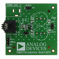
SSM2315-EVALZ
Specifications of SSM2315-EVALZ


Related parts for SSM2315-EVALZ


SSM2315-EVALZ Summary of contents
Page 1
... THD + N driving a 3 Ω load from a single 5.0 V supply. The SSM2315 comes with a differential mode input port and a high efficiency, full H-bridge at the output that enables direct coupling of the audio power signal to the loudspeaker. The differential mode input stage allows for canceling of common- mode noise ...
Page 2
... EVAL-SSM2315 TABLE OF CONTENTS Features .............................................................................................. 1 General Description ......................................................................... 1 Evaluation Board Description ......................................................... 1 Revision History ............................................................................... 2 Evaluation Board Hardware ............................................................ 3 Input Configuration ..................................................................... 3 Output Configuration .................................................................. 3 Power Supply Configuration ....................................................... 3 Component Selection................................................................... 3 REVISION HISTORY 5/09—Revision 0: Initial Version PCB Layout Guidelines .................................................................4 Getting Started ...............................................................................5 What to Test ...................................................................................5 Evaluation Board Schematic and Artwork .....................................6 ...
Page 3
... The SSM2315 does not require any external LC output filters because it has a low noise modulation scheme. However, if the speaker length is >10 cm recommended that a ferrite bead (L1 and L2) be placed near each output pin of the SSM2315 to reduce electromagnetic interference (EMI), as shown in the schematic in Figure 4. ...
Page 4
... GO TO GND PLANE BY VIA GO TO VDD PLANE BY VIA Figure 3. Preferred PCB Layout for the SSM2315 Evaluation Board Layer Stacks and Grounding The stack-up for the evaluation board is a 4-layer structure. • Top layer—component layer with power and output copper land and ground copper pouring. • ...
Page 5
... Component Placement and Clearance Place all related components except decoupling capacitors on the same side as the SSM2315 and as close as possible to the chip to avoid vias (see Figure 5). Place decoupling capacitors on the bottom side and close to the GND pin (see Figure 7). Top Layer Copper Land and Ground Pouring The output peak current of this amplifier is more than 1 A ...
Page 6
... IN+ OUT– C1 100pF B0603 IN– OUT+ U1 SSM2315 C2 2C 100pF SD JP2 HDR1X2 NOTES 1. L3, L4, C7, C8, C9, C10, AND J1 ARE NOT POPULATED. Figure 4. Schematic of the SSM2315 Evaluation Board Rev Page 15µH G1 GAP OUT– 1nF 100pF 1nF JP1 G2 HDR1X2 GAP OUT C10 ...
Page 7
... Figure 5. Top Layer with Top Silkscreen Figure 6. Top Silkscreen Figure 7. Bottom Silkscreen Figure 8. Top Layer Rev Page EVAL-SSM2315 ...
Page 8
... EVAL-SSM2315 Figure 9. Layer 2 (Ground Plane) Figure 10. Layer 3 (Power Plane) Figure 11. Bottom Layer Rev Page ...
Page 9
... R1 100 kΩ resistor Ω resistor, 1/ SSM2315 ORDERING GUIDE Model Description 1 SSM2315-EVALZ Evaluation Board RoHS Compliant Part. ESD CAUTION Rev Page EVAL-SSM2315 Supplier/Part No. AVX, 06035A101KAT2A Kemet, C0603C102J5GACTU Murata, GRM31MF51A106ZA01L Kemet, C0603C104K4RACTU CUI, PJ1-021 CUI, SJ1-3523N Tyco, 4-103747-0-02 ...
Page 10
... EVAL-SSM2315 NOTES Rev Page ...
Page 11
... NOTES Rev Page EVAL-SSM2315 ...
Page 12
... EVAL-SSM2315 NOTES ©2009 Analog Devices, Inc. All rights reserved. Trademarks and registered trademarks are the property of their respective owners. EB07818-0-5/09(0) Rev Page ...