SSM2315-EVALZ Analog Devices Inc, SSM2315-EVALZ Datasheet - Page 3
SSM2315-EVALZ
Manufacturer Part Number
SSM2315-EVALZ
Description
BOARD EVAL SSM2315
Manufacturer
Analog Devices Inc
Specifications of SSM2315-EVALZ
Amplifier Type
Class D
Output Type
1-Channel (Mono)
Max Output Power X Channels @ Load
4.28W x 1 @ 3 Ohm
Voltage - Supply
2.5 V ~ 5.5 V
Operating Temperature
-40°C ~ 85°C
Board Type
Fully Populated
Utilized Ic / Part
SSM2315
Silicon Manufacturer
Analog Devices
Application Sub Type
Audio Power Amplifier - Class D
Kit Application Type
Amplifier
Silicon Core Number
SSM2315
Kit Contents
Board
Lead Free Status / RoHS Status
Lead free / RoHS Compliant


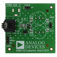
EVALUATION BOARD HARDWARE
INPUT CONFIGURATION
On the left side of the board below the power jack, there is a
standard 3.5 mm audio stereo jack connector, J2 (see Figure 1).
Below J2 is a 3-pin header (JP4). These headers are used to feed the
audio signal into the board.
If the input audio signal is differential (IN+ and IN−), use either
J2 or JP4. In this case, all three pins of JP4 are used for IN+,
IN−, and the ground.
For a single-ended audio input, using JP4 as the input connector is
recommended. In this case, only two pins of JP4 are used: one
pin is for the ground and the other is for either IN+ or IN−. If
IN+ is used, place a jumper between Pin 2 and Pin 3 of JP4,
shorting IN− to ground. If IN− is used, place the jumper
between Pin 1 and Pin 2 of JP4, connecting IN+ to ground.
The two-pin header, JP2, is used to turn the SSM2315 amplifier
on and off. Putting a jumper on JP2 shuts down the SSM2315 so
that only a minimum current (about 20 nA) is drawn from the
power supply. Removing the jumper puts the SSM2315 in normal
operating mode.
OUTPUT CONFIGURATION
The output connector, JP1, is located on the right side of the
board. JP1 drives a loudspeaker whose impedance should be
no less than 3 Ω.
The SSM2315 does not require any external LC output filters
because it has a low noise modulation scheme. However, if the
speaker length is >10 cm, it is recommended that a ferrite bead
(L1 and L2) be placed near each output pin of the SSM2315 to
reduce electromagnetic interference (EMI), as shown in the
schematic in Figure 4.
On the board, there are two inductors, L3 and L4, that are not
loaded and are not required for normal operation (they are shorted
by the solder gaps, G1 and G2). Some users may want to add these
inductors to evaluate certain applications with tighter EMI vs.
audio performance constraints. If L3 and L4 are loaded, the
solder on G1 and G2 must be removed with a soldering iron.
As an aid, a properly tuned ferrite bead based EMI filter is
assembled at the output terminals of the device. For optimal
performance, as specified in the SSM2315 data sheet (in
particular, for THD and SNR), remove the entire EMI filter,
short across the ferrite bead terminals, and open the capacitor
terminals.
Rev. 0 | Page 3 of 12
POWER SUPPLY CONFIGURATION
The schematic for the evaluation board is shown in Figure 4.
There is a PCB footprint to populate a standard power jack (J1),
which accepts a 2.5 V to 5.5 V dc power supply (see the upper
left corner of Figure 1). For most laboratory measurement
setups, use the 2-pin header (JP3) to power the board. In either
case, care must be taken to connect the dc power with correct
polarity and voltage. The J1 jack is not populated during PCB
assembly.
Polarity and Voltage
The wrong power supply polarity or overvoltage may perma-
nently damage the board. The maximum peak current is
approximately 0.33 A when driving an 8 Ω load and when
the input voltage is 5 V.
COMPONENT SELECTION
Selecting the proper components is the key to achieving the
performance required at the cost budgeted.
Input Coupling Capacitor Selection—C11 and C12
The input capacitors, C11 and C12, should be large enough to
couple the low frequency signal components in the incoming
signal but small enough to filter out unnecessary low frequency
signals. For music signals, the cutoff frequency chosen is often
between 20 Hz and 30 Hz. The value of the input capacitor is
calculated by
where:
R = 80 kΩ + R
desired gain; on the schematic (see Figure 4), this is the 0 Ω
resistor at the input pins).
f
Output Ferrite Beads—L1 and L2
The L1 and L2 output beads are necessary components for
filtering out the EMI caused at the switching output nodes
when the length of the speaker wire is greater than 10 cm. The
penalty for using ferrite beads for EMI filtering is slightly worse
noise and distortion performance at the system level due to the
nonlinearity of the beads.
Ensure that these beads have enough current conducting
capability while providing sufficient EMI attenuation. The
current rating needed for an 8 Ω load is approximately 420 mA,
and impedance at 100 MHz must be ≥120 Ω. In addition, the
lower the dc resistance (DCR) of these beads, the better for
minimizing their power consumption.
Table 1 describes the recommended beads.
c
is the cutoff frequency.
C = 1/(2πRf
EXT
c
)
(the external resistor used to fine-tune the
EVAL-SSM2315
Related parts for SSM2315-EVALZ
Image
Part Number
Description
Manufacturer
Datasheet
Request
R

Part Number:
Description:
±1.7g Dual-Axis IMEMS Accelerometer Evaluation Board
Manufacturer:
Analog Devices Inc
Datasheet:

Part Number:
Description:
Inertial Sensor Evaluation System
Manufacturer:
Analog Devices Inc
Datasheet:
Part Number:
Description:
Manufacturer:
Analog Devices Inc
Datasheet:
Part Number:
Description:
Manufacturer:
Analog Devices Inc
Datasheet:
Part Number:
Description:
Manufacturer:
Analog Devices Inc
Datasheet:
Part Number:
Description:
Manufacturer:
Analog Devices Inc
Datasheet:
Part Number:
Description:
Manufacturer:
Analog Devices Inc
Datasheet:
Part Number:
Description:
Manufacturer:
Analog Devices Inc
Datasheet:
Part Number:
Description:
Manufacturer:
Analog Devices Inc
Datasheet:
Part Number:
Description:
Manufacturer:
Analog Devices Inc
Datasheet:
Part Number:
Description:
Manufacturer:
Analog Devices Inc
Datasheet:
Part Number:
Description:
Manufacturer:
Analog Devices Inc
Datasheet:
Part Number:
Description:
Manufacturer:
Analog Devices Inc
Datasheet: