SSM2315-EVALZ Analog Devices Inc, SSM2315-EVALZ Datasheet - Page 4
SSM2315-EVALZ
Manufacturer Part Number
SSM2315-EVALZ
Description
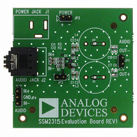
BOARD EVAL SSM2315
Manufacturer
Analog Devices Inc
Specifications of SSM2315-EVALZ
Amplifier Type
Class D
Output Type
1-Channel (Mono)
Max Output Power X Channels @ Load
4.28W x 1 @ 3 Ohm
Voltage - Supply
2.5 V ~ 5.5 V
Operating Temperature
-40°C ~ 85°C
Board Type
Fully Populated
Utilized Ic / Part
SSM2315
Silicon Manufacturer
Analog Devices
Application Sub Type
Audio Power Amplifier - Class D
Kit Application Type
Amplifier
Silicon Core Number
SSM2315
Kit Contents
Board
Lead Free Status / RoHS Status
Lead free / RoHS Compliant


EVAL-SSM2315
Table 1. Recommended Output Beads (L1 and L2)
Part No.
BLM18PG121SN1D
MPZ1608S101A
MPZ1608S221A
BLM18EG221SN1D
Table 2. Recommended Output Inductors (L3 and L4)
Part No.
LQM31PNR47M00
LQM31PN1R0M00
LQM21PNR47MC0
LQM21PN1R0MC0
LQH32CN2R2M53
Output Shunting Capacitors
There are two groups of output shunting capacitors: C1, C2, C3,
and C4 work with the L1 and L2 ferrite beads; C7, C8, C9, and
C10 work with L3 and L4, if they are used. Use small size (0603
or 0402) multilayer ceramic capacitors that are made of X7R or
COG (NPO) materials. Note that the capacitors can be used in
pairs: a capacitor with small capacitance (up to 100 pF) plus a
capacitor with a larger capacitance (less than 1 nF). This config-
uration provides thorough EMI reduction for the entire frequency
spectrum. For BOM cost reduction and capable performance,
a single capacitor of approximately 470 pF can be used.
Output Inductors—L3 and L4
If you prefer using inductors for the purpose of EMI filtering
at the output nodes, choose inductance that is < 2.2 μH. The
higher the inductance, the lower the EMI is at the output.
However, the cost and power consumption by the inductors
are higher. Using 0.47 μH to 2.2 μH inductors is recom-mended,
and the current rating needs >600 mA (saturation current) for
an 8 Ω load. Table 2 shows the recommended inductors. Note
that these inductors are not populated on the evaluation board.
PCB LAYOUT GUIDELINES
To keep the EMI under the allowable limit and to ensure that
the amplifier chip operates under the temperature limit, PCB
layout is critical in application design. Figure 3 shows the
preferred layout for the SSM2315 evaluation board.
Manufacturer
Murata
TDK
TDK
Murata
Manufacturer
Murata
Murata
Murata
Murata
Murata
Rev. 0 | Page 4 of 12
Z (Ω)
120
100
220
220
0.47
0.47
L (μH)
1.0
1.0
2.2
Layer Stacks and Grounding
The stack-up for the evaluation board is a 4-layer structure.
•
•
•
•
Top layer—component layer with power and output copper
land and ground copper pouring.
Second layer—dedicated ground plane.
Third layer—dedicated power plane.
Bottom layer—bottom layer with ground copper pouring.
I
1400
1200
1100
800
790
I
2000
3000
2000
2000
Figure 3. Preferred PCB Layout for the SSM2315 Evaluation Board
MAX
MAX
GO TO VDD PLANE BY VIA
(mA)
(mA)
GO TO GND PLANE
BY VIA
0.05
0.03
0.05
0.05
DCR (Ω)
0.07
0.12
0.12
0.19
0.1
DCR (Ω)
VIA SIZE SHOULD BE
AS LARGE AS POSSIBLE
GO TO GND PLANE BY VIA
Size (mm)
1.6 × 0.8 × 0.8
1.6 × 0.8 × 0.8
1.6 × 0.8 × 0.8
1.6 × 0.8 × 0.8
Size (mm)
3.2 × 1.6 × 0.85
3.2 × 1.6 × 0.85
2.0 × 1.25 × 0.5
2.0 × 1.25 × 0.5
3.2 × 2.5 × 1.55
Related parts for SSM2315-EVALZ
Image
Part Number
Description
Manufacturer
Datasheet
Request
R

Part Number:
Description:
±1.7g Dual-Axis IMEMS Accelerometer Evaluation Board
Manufacturer:
Analog Devices Inc
Datasheet:

Part Number:
Description:
Inertial Sensor Evaluation System
Manufacturer:
Analog Devices Inc
Datasheet:
Part Number:
Description:
Manufacturer:
Analog Devices Inc
Datasheet:
Part Number:
Description:
Manufacturer:
Analog Devices Inc
Datasheet:
Part Number:
Description:
Manufacturer:
Analog Devices Inc
Datasheet:
Part Number:
Description:
Manufacturer:
Analog Devices Inc
Datasheet:
Part Number:
Description:
Manufacturer:
Analog Devices Inc
Datasheet:
Part Number:
Description:
Manufacturer:
Analog Devices Inc
Datasheet:
Part Number:
Description:
Manufacturer:
Analog Devices Inc
Datasheet:
Part Number:
Description:
Manufacturer:
Analog Devices Inc
Datasheet:
Part Number:
Description:
Manufacturer:
Analog Devices Inc
Datasheet:
Part Number:
Description:
Manufacturer:
Analog Devices Inc
Datasheet:
Part Number:
Description:
Manufacturer:
Analog Devices Inc
Datasheet: