DAK-85 Power Integrations, DAK-85 Datasheet - Page 14
DAK-85
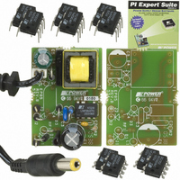
Manufacturer Part Number
DAK-85
Description
DESIGN ACCELERATOR KIT LP SWITCH
Manufacturer
Power Integrations
Series
LinkSwitch®-LPr
Specifications of DAK-85
Main Purpose
AC/DC, Primary Side
Outputs And Type
1, Isolated
Power - Output
2W
Voltage - Output
6V
Current - Output
330mA
Voltage - Input
90 ~ 265VAC
Regulator Topology
Flyback
Frequency - Switching
66kHz
Board Type
Bare (Unpopulated) and Fully Populated
Utilized Ic / Part
LNK562, LNK563, LNK564
Lead Free Status / RoHS Status
Lead free / RoHS Compliant
Other names
596-1104
Available stocks
Company
Part Number
Manufacturer
Quantity
Price
Company:

Part Number:
DAK-85
Manufacturer:
Power Integrations
Quantity:
135


7.5 Design Spreadsheet
ENTER APPLICATION VARIABLES
VACMIN
VACMAX
fL
VO
IO
Constant Voltage / Constant
Current Output
Output Cable Resistance
PO
Feedback Type
Add Bias Winding
Clampless design
n
Z
tC
CIN
Input Rectification Type
ENTER LinkSwitch-LP VARIABLES
LinkSwitch-LP
Chosen Device
ILIMITMIN
ILIMITMAX
fSmin
I^2fMIN
I^2fTYP
VOR
VDS
VD
KP
ENTER TRANSFORMER CORE/CONSTRUCTION VARIABLES
Core Type
Core
Bobbin
AE
LE
AL
BW
M
L
NS
NB
VB
R1
LP_091605; Rev.1.0;
ACDC_LinkSwitch-
Integrations 2005
Copyright Power
Power Integrations
Tel: +1 408 414 9200 Fax: +1 408 414 9201
www.powerint.com
LNK564
INPUT
10.00
88.00
BIAS
6.00
0.33
YES
0.05
YES
YES
0.70
0.50
2.80
265
90
50
H
8
LNK564
EE16_BOBBIN P/N:
INFO
EE16
OUTP
Clamp
CVCC
93000 Hertz
0.124 Amps
0.146 Amps
EE16
0.192 cm^2
21.93 Volts
36.89 k-ohms
UT
1665 A^2Hz
1850 A^2Hz
1140 nH/T^2
0.05
1.99
1.54
less
Yes
0.5
0.5 Volts
3.5 cm
8.6 mm
88 Volts
10 Volts
27
Bias Winding Enter 'BIAS' for Bias winding feedback and 'OPTO' for
H
0 mm
2
8
UNIT
Volts
Volts
Hertz
Volts
Amps
Volts
Ohms
Watts
mSecond
s
uFarads
P/N:
ACDC_LinkSwitch-LP_091605_Rev1-0.xls; LinkSwitch-LP
Continuous/Discontinuous Flyback Transformer Design
Spreadsheet
EP85 Design
Minimum AC Input Voltage
Maximum AC Input Voltage
AC Mains Frequency
Output Voltage (main) measured at the end of output cable (For
CV/CC designs enter typical CV tolerance limit)
Power Supply Output Current (For CV/CC designs enter typical
CC tolerance limit)
Enter "YES" for CV/CC output. Enter "NO" for CV only output
Enter the resistance of the output cable (if used)
Output Power (VO x IO + dissipation in output cable)
Optocoupler feedback
Enter 'YES' to add a Bias winding. Enter 'NO' to continue
design without a Bias winding. Addition of Bias winding can
lower no load consumption
Enter 'YES' for a clampless design. Enter 'NO' if an external
clamp circuit is used.
Efficiency Estimate at output terminals. For CV only designs
enter 0.7 if no better data available
Loss Allocation Factor (Secondary side losses / Total losses)
Bridge Rectifier Conduction Time Estimate
Input Capacitance
Choose H for Half Wave Rectifier and F for Full Wave
Rectification
LinkSwitch-LP device
Minimum Current Limit
Maximum Current Limit
Minimum Device Switching Frequency
I^2f Minimum value (product of current limit squared and
frequency is trimmed for tighter tolerance)
I^2f typical value (product of current limit squared and
frequency is trimmed for tighter tolerance)
Reflected Output Voltage
LinkSwitch-LP on-state Drain to Source Voltage
Output Winding Diode Forward Voltage Drop
Ripple to Peak Current Ratio (0.9<KRP<1.0 : 1.0<KDP<6.0)
Suggested smallest commonly available core
PC40EE16-Z
EE16_BOBBIN
Core Effective Cross Sectional Area
Core Effective Path Length
Ungapped Core Effective Inductance
Bobbin Physical Winding Width
Safety Margin Width (Half the Primary to Secondary Creepage
Distance)
Number of primary layers
Number of Secondary Turns
Number of Bias winding turns
Bias Winding Voltage
Resistor divider component between bias wiinding and FB pin
of LinkSwitch-LP
Page 14 of 32
Related parts for DAK-85
Image
Part Number
Description
Manufacturer
Datasheet
Request
R

Part Number:
Description:
KIT DESIGN ACCELERATOR MODEM
Manufacturer:
Power Integrations
Datasheet:

Part Number:
Description:
KIT DESIGN ACCELERATOR SET TOP
Manufacturer:
Power Integrations
Datasheet:

Part Number:
Description:
KIT REF DES DPA 6.6W DC-DC CONV
Manufacturer:
Power Integrations
Datasheet:

Part Number:
Description:
KIT DESIGN ACCELERATOR POE CONV
Manufacturer:
Power Integrations
Datasheet:

Part Number:
Description:
DESIGN ACCELERATOR KIT XT SWITCH
Manufacturer:
Power Integrations
Datasheet:

Part Number:
Description:
KIT DESIGN ACC PEAKSWITCH FAMILY
Manufacturer:
Power Integrations
Datasheet:

Part Number:
Description:
KIT DESIGN ACCELERATOR ADAPTER
Manufacturer:
Power Integrations
Datasheet:

Part Number:
Description:
KIT DESIGN ACCELERATOR ADAPTER
Manufacturer:
Power Integrations
Datasheet:

Part Number:
Description:
KIT DESIGN ACCELERATOR DC-DC
Manufacturer:
Power Integrations
Datasheet:

Part Number:
Description:
KIT DESIGN ACCELERATOR DPA SW
Manufacturer:
Power Integrations
Datasheet: