STEVAL-ISA025V1 STMicroelectronics, STEVAL-ISA025V1 Datasheet - Page 35
STEVAL-ISA025V1
Manufacturer Part Number
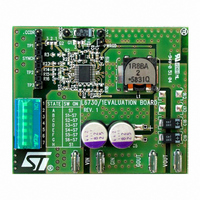
STEVAL-ISA025V1
Description
EVAL BOARD 30A 400KHZ L6730
Manufacturer
STMicroelectronics
Type
DC/DC Switching Converters, Regulators & Controllersr
Specifications of STEVAL-ISA025V1
Design Resources
STEVAL-ISA025V1 Gerber Files STEVAL-ISA025V1 Schematic STEVAL-ISA025V1 Bill of Materials
Main Purpose
DC/DC, Step Down
Outputs And Type
1, Non-Isolated
Voltage - Output
3.3V
Current - Output
30A
Voltage - Input
4.5 ~ 14V
Regulator Topology
Buck
Frequency - Switching
400kHz
Board Type
Fully Populated
Utilized Ic / Part
L6730
Input Voltage
4.5 V to 14 V
Output Voltage
3.3 V
Product
Power Management Modules
Silicon Manufacturer
ST Micro
Silicon Core Number
L6730
Kit Application Type
Power Management - Voltage Regulator
Rohs Compliant
No
Lead Free Status / RoHS Status
Lead free / RoHS Compliant
Power - Output
-
Lead Free Status / Rohs Status
Lead free / RoHS Compliant
For Use With/related Products
L6730
Other names
497-5868
Available stocks
Company
Part Number
Manufacturer
Quantity
Price
Company:

Part Number:
STEVAL-ISA025V1
Manufacturer:
STMicroelectronics
Quantity:
1


L6730 - L6730B
6.4
Compensation network
The loop is based on a voltage mode control
the internal/external reference voltage and scaled by the external resistor divider. The error
amplifier output V
pulse-width modulated (PWM) with an amplitude of V
is filtered by the output filter. The modulator transfer function is the small signal transfer
function of V
L-Cout resonance and a zero at F
Gain of the modulator is simply the input voltage V
voltage: V
Figure 29. Compensation network
The compensation network consists in the internal error amplifier, the impedance networks
Z
provide a closed loop transfer function with the highest 0dB crossing frequency to have
fastest transient response (but always lower than fsw/10) and the highest gain in DC
conditions to minimize the load regulation error. A stable control loop has a gain crossing the
IN
(R3, R4 and C20) and Z
OSC
OUT
.
/V
COMP
COMP
. This function has a double pole at frequency F
is then compared with the oscillator triangular wave to provide a
FB
Doc ID 11938 Rev 3
(R5, C18 and C19). The compensation network has to
Z
ESR
FB
depending on the output capacitor’s ESR. The DC
(Figure
IN
29). The output voltage is regulated to
divided by the peak-to-peak oscillator
IN
at the PHASE node. This waveform
Z
IN
LC
Application details
depending on the
35/52
Related parts for STEVAL-ISA025V1
Image
Part Number
Description
Manufacturer
Datasheet
Request
R

Part Number:
Description:
BOARD RGB CTR ST7,STP08C596MTR
Manufacturer:
STMicroelectronics
Datasheet:

Part Number:
Description:
Power Management IC Development Tools Full Speed USB to RS232 Bridge Demo
Manufacturer:
STMicroelectronics
Datasheet:
Part Number:
Description:
Power Management IC Development Tools 2.5W solar eval BRD USB SPV1040 LD39050
Manufacturer:
STMicroelectronics
Datasheet:

Part Number:
Description:
BOARD EVAL FOR MEMS SENSORS
Manufacturer:
STMicroelectronics
Datasheet:

Part Number:
Description:
KIT DEV STARTER ST10F276Z5
Manufacturer:
STMicroelectronics
Datasheet:

Part Number:
Description:
BOARD EVAL HDMI $ VIDEO SWITCH
Manufacturer:
STMicroelectronics
Datasheet:

Part Number:
Description:
BOARD DEMO ACCELEROMETER DIL24
Manufacturer:
STMicroelectronics
Datasheet:

Part Number:
Description:
BOARD STLM75/STDS75/ST72F651
Manufacturer:
STMicroelectronics
Datasheet:

Part Number:
Description:
EVAL BOARD 3AXIS MEMS ACCELLRMTR
Manufacturer:
STMicroelectronics
Datasheet:

Part Number:
Description:
BOARD EVAL 8BIT MICRO + TDE1708
Manufacturer:
STMicroelectronics
Datasheet:
Part Number:
Description:
STMicroelectronics [RIPPLE-CARRY BINARY COUNTER/DIVIDERS]
Manufacturer:
STMicroelectronics
Datasheet:
Part Number:
Description:
STMicroelectronics [LIQUID-CRYSTAL DISPLAY DRIVERS]
Manufacturer:
STMicroelectronics
Datasheet:
Part Number:
Description:
BOARD EVAL FOR MEMS SENSORS
Manufacturer:
STMicroelectronics
Datasheet: