STEVAL-ISA025V1 STMicroelectronics, STEVAL-ISA025V1 Datasheet - Page 43
STEVAL-ISA025V1
Manufacturer Part Number
STEVAL-ISA025V1
Description
EVAL BOARD 30A 400KHZ L6730
Manufacturer
STMicroelectronics
Type
DC/DC Switching Converters, Regulators & Controllersr
Specifications of STEVAL-ISA025V1
Design Resources
STEVAL-ISA025V1 Gerber Files STEVAL-ISA025V1 Schematic STEVAL-ISA025V1 Bill of Materials
Main Purpose
DC/DC, Step Down
Outputs And Type
1, Non-Isolated
Voltage - Output
3.3V
Current - Output
30A
Voltage - Input
4.5 ~ 14V
Regulator Topology
Buck
Frequency - Switching
400kHz
Board Type
Fully Populated
Utilized Ic / Part
L6730
Input Voltage
4.5 V to 14 V
Output Voltage
3.3 V
Product
Power Management Modules
Silicon Manufacturer
ST Micro
Silicon Core Number
L6730
Kit Application Type
Power Management - Voltage Regulator
Rohs Compliant
No
Lead Free Status / RoHS Status
Lead free / RoHS Compliant
Power - Output
-
Lead Free Status / Rohs Status
Lead free / RoHS Compliant
For Use With/related Products
L6730
Other names
497-5868
Available stocks
Company
Part Number
Manufacturer
Quantity
Price
Company:

Part Number:
STEVAL-ISA025V1
Manufacturer:
STMicroelectronics
Quantity:
1


L6730 - L6730B
8
I/O Description
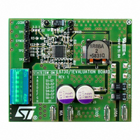
Figure 38. Demonstration board
Table 11.
Output (V
Input (Vin-Gin)
V
CC
Symbol
V
-GND
TP1
CCDR
OUT
-G
I/O functions
CC
OUT
)
The input voltage can range from 1.8V to 14V. If the input voltage is between
4.5V and 14V it can supply also the device (through the V
case the pin 1 and 2 of the jumper G1 must be connected together.
The output voltage is fixed at 3.3V but it can be changed by replacing the
resistor R14 of the output resistor divider:
The over-current-protection limit is set at 15A but it can be changed by
replacing the resistors R1 and R12 (see OCL and OCH pin in
connection).
Using the input voltage to supply the controller no power is required at this
input. However the controller can be supplied separately from the power stage
through the V
open.
An internal LDO provides the power into the device. The input of this stage is
the V
providing directly a 5V voltage from V
and 3 of the jumper G1 must be shorted.
This pin can be used as an input or as a test point. If all the jumper G2 pins are
shorted, TP1 can be used as a test point of the voltage at the EAREF pin. If
the pins 2 and 3 of G2 are connected together, TP1 can be used as an input to
provide an external reference for the internal error amplifier (see section 4.3.
Internal and external references).
CC
pin and the output (5V) is the V
Doc ID 11938 Rev 3
CC
input (4.5-14V) and, in this case, jumper G1 must be left
Vo
=
V
REF
Function
⋅
CCDR
1 (
CCDR
+
R
R
and Gndcc. In this case the pins 1
16
14
)
pin. The LDO can be bypassed,
CC
pin) and in this
I/O Description
Table 4: Pin
43/52
Related parts for STEVAL-ISA025V1
Image
Part Number
Description
Manufacturer
Datasheet
Request
R

Part Number:
Description:
BOARD RGB CTR ST7,STP08C596MTR
Manufacturer:
STMicroelectronics
Datasheet:

Part Number:
Description:
Power Management IC Development Tools Full Speed USB to RS232 Bridge Demo
Manufacturer:
STMicroelectronics
Datasheet:
Part Number:
Description:
Power Management IC Development Tools 2.5W solar eval BRD USB SPV1040 LD39050
Manufacturer:
STMicroelectronics
Datasheet:

Part Number:
Description:
BOARD EVAL FOR MEMS SENSORS
Manufacturer:
STMicroelectronics
Datasheet:

Part Number:
Description:
KIT DEV STARTER ST10F276Z5
Manufacturer:
STMicroelectronics
Datasheet:

Part Number:
Description:
BOARD EVAL HDMI $ VIDEO SWITCH
Manufacturer:
STMicroelectronics
Datasheet:

Part Number:
Description:
BOARD DEMO ACCELEROMETER DIL24
Manufacturer:
STMicroelectronics
Datasheet:

Part Number:
Description:
BOARD STLM75/STDS75/ST72F651
Manufacturer:
STMicroelectronics
Datasheet:

Part Number:
Description:
EVAL BOARD 3AXIS MEMS ACCELLRMTR
Manufacturer:
STMicroelectronics
Datasheet:

Part Number:
Description:
BOARD EVAL 8BIT MICRO + TDE1708
Manufacturer:
STMicroelectronics
Datasheet:
Part Number:
Description:
STMicroelectronics [RIPPLE-CARRY BINARY COUNTER/DIVIDERS]
Manufacturer:
STMicroelectronics
Datasheet:
Part Number:
Description:
STMicroelectronics [LIQUID-CRYSTAL DISPLAY DRIVERS]
Manufacturer:
STMicroelectronics
Datasheet:
Part Number:
Description:
BOARD EVAL FOR MEMS SENSORS
Manufacturer:
STMicroelectronics
Datasheet: