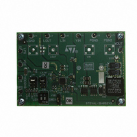
STEVAL-ISA052V2 STMicroelectronics, STEVAL-ISA052V2 Datasheet
STEVAL-ISA052V2
Specifications of STEVAL-ISA052V2
Available stocks


Related parts for STEVAL-ISA052V2


STEVAL-ISA052V2 Summary of contents
Page 1
Features ■ Switching section – 4 input voltage range – 0.6 V, ±1 % voltage reference – Selectable 1.5 V fixed output voltage – Adjustable 0 3.3 V output voltage – 1.237 V ±1 ...
Page 2
Contents Contents 1 Typical application circuit . . . . . . . . . . . . . . . . . . . . . . . . . . . . . . . . . . ...
Page 3
PM6675AS 7.1.12 7.2 LDO linear regulator section . . . . . . . . . . . . . . . . . . . . . . . . . . . . . . . . . ...
Page 4
Typical application circuit 1 Typical application circuit Figure 1. Application circuit V V LDOIN LDOIN 10 10 VSEL VSEL IN4 IN4 IN4 23 23 LIN LIN LDO PG LDO LPG LPG 24 24 LOUT ...
Page 5
PM6675AS 2 Pin settings 2.1 Connections Figure 2. Pin connection (through top view) NOSKIP NOSKIP NOSKIP LGND LGND LGND LFB LFB LFB PM6675A PM6675A PM6675A PM6675A PM6675AS LPG LPG LPG SGND SGND ...
Page 6
Pin settings 2.2 Pin description Table 2. Pin functions N° Pin 1 LGND 2 LFB 3 NOSKIP 4 LPG 5 SGND 6 AVCC 7 VREF 8 VOSC 9 VSNS 10 VSEL 11 COMP 12 LILIM 13 SWEN 14 LEN 15 ...
Page 7
PM6675AS Table 2. Pin functions (continued) N° Pin 19 CSNS 20 PHASE 21 HGATE 22 BOOT 23 LIN 24 LOUT Current sense input for the switching section. This pin must be connected through a resistor to the drain of the ...
Page 8
Electrical data 3 Electrical data 3.1 Maximum rating Table 3. Absolute maximum ratings Symbol V AVCC to SGND AVCC V VCC to SGND VCC PGND, LGND to SGND HGATE and BOOT to PHASE HGATE and BOOT to PGND V PHASE ...
Page 9
PM6675AS 4 Electrical characteristics Table 6. Electrical characteristics ° °C , VCC = AVCC = +5 V, LIN = 1.5 V and LOUT= 0 not otherwise A (1) specified . Symbol Parameter ...
Page 10
Electrical characteristics Table 6. Electrical characteristics (continued -25 ° °C , VCC = AVCC = +5 V, LIN = 1.5 V and LOUT= 0 not otherwise A (1) specified. Symbol Parameter Current limit and ...
Page 11
PM6675AS Table 6. Electrical characteristics (continued -25 ° °C , VCC = AVCC = +5 V, LIN = 1.5 V and LOUT= 0 not otherwise A (1) specified. Symbol Parameter LDO sink current limit ...
Page 12
Block diagram 5 Block diagram Figure 3. Functional and block diagram 0.6V LFB LFB LFB LIN LIN LIN LOUT LOUT LOUT LDS LDS LGND LGND Vr +10 Vr +10 Vr +10 LPG ...
Page 13
PM6675AS 6 Typical operating characteristics Figure 4. Efficiency vs output load F = 330 kHz VOUT=1 VIN = 24 V VOUT - Efficiency 100 0.001 0.010 0.100 Current ...
Page 14
Typical operating characteristics Figure 10. VOUT = 1.5V , VIN = 24V, IVOUT = 0 A, forced-PWM mode Figure 12. VOUT Soft-start @150mΩ load, pulse-skip mode Figure 14. VOUT Load Transient (VIN = 24 V, LOAD = 0 A -> ...
Page 15
PM6675AS Figure 16. VOUT and LOUT output voltages. VOUT soft-end. LOUT powered by an auxiliary rail Figure 18. UV protection, pulse-skip mode LOUT powered by an auxiliary rail Figure 20. VOUT current limit protection during a load transient (0 A ...
Page 16
Device description 7 Device description The PM6675AS combines a single high efficiency step-down controller and an independent Low Drop-Out (LDO) linear regulator in the same package. The switching controller section is a high-performance, pseudo-fixed frequency, Constant- On-Time (COT) based regulator ...
Page 17
PM6675AS The Off-Time duration is solely determined by the output voltage: when lower than the set value (i.e. the voltage at VSNS pin is lower than the internal reference = 0.6 V), the synchronous rectifier is turned off and a ...
Page 18
Device description Referring to the typical application schematic (fig. 1 and 23), the final expression is then: Figure 23. Switching frequency selection and VOSC pin Equation 5 Even if the switching frequency is theoretically independent from input and output voltages, ...
Page 19
PM6675AS Figure 24. Switching section simplified block diagram ...
Page 20
Device description Figure 25. Circuitry for output ripple compensation COMP PIN VOLTAGE Vr t OUTPUT VOLTAGE t The additional capacitor is used to reduce the voltage on the COMP pin when higher than 300 mVpp and is unnecessary for most ...
Page 21
PM6675AS where fixed design parameter (k > 3). It determinates the minimum integrator capacitor value: Equation 7 where µs is the integrator transconductance. If the ripple on the COMP pin is greater than the ...
Page 22
Device description Figure 26. "Virtual-ESR" network T NODE VOLTAGE Δ OUTPUT VOLTAGE The ripple on the COMP pin is the sum of the output voltage ripple and the triangular ripple generated by the Virtual-ESR Network. In fact the ...
Page 23
PM6675AS and Equation 13 Moreover, the C INT Equation 14 where R is the sum of the ESR of the output capacitor and the equivalent ESR given by TOT the Virtual-ESR Network (R determines the minimum integrator capacitor value C ...
Page 24
Device description 7.1.3 Pulse-skip and no-audible pulse-skip modes High efficiency at light load conditions is achieved by PM6675AS entering the Pulse-Skip Mode (if enabled). At light load conditions the zero-crossing comparator truncates the low- side switch On-Time as soon as ...
Page 25
PM6675AS No-audible pulse-skip mode Some audio-noise sensitive applications cannot accept the switching frequency to enter the audible range as is possible in Pulse-Skip mode with very light loads. For this reason, the PM6675AS implements an additional feature to maintain a ...
Page 26
Device description 7.1.4 Mode-of-operation selection Figure 29. VSEL and NOSKIP multifunction pin configurations The PM6675AS has been designed to satisfy the widest range of applications. The device is provided of some multilevel pins which allow the user to choose the ...
Page 27
PM6675AS 7.1.5 Current sensing and current limit The PM6675AS switching controller employes a valley current sensing algorithm to properly handle the current limit protection and the inductor current zero-crossing information. The current is sensed during the conduction time of the ...
Page 28
Device description 7.1.6 POR, UVLO and soft-start The PM6675AS automatically performs an internal startup sequence during the rising phase of the analog supply of the device (AVCC). The switching controller remains in a stand-by state until AVCC crosses the upper ...
Page 29
PM6675AS Figure 32. Soft-start at heavy load (a) and short-circuit (b) condition, pulse-skip enabled 7.1.7 Switching section power-good signal The SPG pin is an open drain output used to monitor output voltage through VSNS (in fixed output voltage mode) or ...
Page 30
Device description 7.1.9 Gate drivers The integrated high-current gate drivers allow using different power MOSFETs. The high- side driver employes a bootstrap circuit which is supplied by the +5 V rail. The BOOT and PHASE pins work respectively as supply ...
Page 31
PM6675AS The Under-Voltage Protection circuit is enabled only at the end of the soft-start. Once an UVP has taken part, a toggle on SWEN pin or a Power-On-Reset is necessary to clear the fault state and restart the section. 7.1.12 ...
Page 32
Device description Figure 34. LDO output voltage selection A compensation capacitor Cc must be added to adjust the dynamic response of the loop. The value calculated according to the desired bandwidth of the LDO regulator and depends ...
Page 33
PM6675AS Figure 36. LDO current limit setting 2.2 2.0 1.8 1.6 1.4 1.2 1.0 0.8 0.6 0.4 0.2 0.0 0.0 0.5 7.2.2 LDO section soft-start The LDO section soft-start is performed by clamping the current limit. During startup, the LDO ...
Page 34
Application information 8 Application information The purpose of this chapter is to show the design procedure of the switching section. The design starts from three main specifications: ● The input voltage range, provided by the battery or the AC adapter. ...
Page 35
PM6675AS Equation 28 a Equation 28 b Referring to the typical application schematic (figs. 1 and 23), the final expression is then: Equation 29 Even if the switching frequency is theoretically independent from battery and output voltages, parasitic parameters involved ...
Page 36
Application information With these considerations, the inductance value can be calculated with the following expression: Equation 30 where f is the switching frequency the inductor current ripple. Once the inductor value is determined, the inductor current ripple ...
Page 37
PM6675AS In Pulse-Skip Mode, low inductance values produce a better efficiency versus load curve, while higher values result in higher full-load efficiency because of the smaller current ripple. 8.1.2 Input capacitor selection In a buck topology converter the current that ...
Page 38
Application information 8.1.3 Output capacitor selection Using tantalum or electrolytic capacitors, the selection is made referring to ESR and voltage rating rather than by a specific capacitance value. The output capacitor has to satisfy the output voltage ripple requirements. At ...
Page 39
PM6675AS In Table 13 some tested polymer capacitors are listed. Table 13. Evaluated output capacitors Manufacturer SANYO HITACHI 8.1.4 MOSFETs selection In SMPS converters, power management efficiency is a high level requirement, so the power dissipation on the power switches ...
Page 40
Application information Table 14. Evaluated high-side MOSFETs Manufacturer ST STS12NH3LL buck converters the power dissipation of the synchronous MOSFET is mainly due to conduction losses: Equation 43 Maximum conduction losses occur at the maximum input voltage: Equation ...
Page 41
PM6675AS 8.1.5 Diode selection A rectifier across the synchronous switch is recommended. The rectifier works as a voltage clamp across the synchronous rectifier and reduces the negative inductor swing during the dead time between turning the high-side MOSFET off and ...
Page 42
Application information where R is the drain-source on-resistance low-side switch. Consider the temperature DSon effect and the worst case value in R The accuracy of the valley current also depends on the offset of the internal comparator (±6 mV). The ...
Page 43
PM6675AS where free design parameter greater than unity (k > determinates the minimum integrator capacitor value C Equation 49 If the ripple on pin COMP is greater than the integrator output dynamic (150 mV), ...
Page 44
Application information Select C as shown: Equation 52 Then calculate R in order to have enough ripple voltage on the integrator input: Equation 53 Where R is the new virtual output capacitor ESR. A good trade-off is to consider an ...
Page 45
PM6675AS 9 Package mechanical data In order to meet environmental requirements, ST offers these devices in ECOPACK packages. These packages have a Lead-free second level interconnect. The category of second Level Interconnect is marked on the package and on the ...
Page 46
Package mechanical data Figure 41. Package dimensions 46/48 PM6675AS ...
Page 47
PM6675AS 10 Revision history Table 19. Document revision history Date 19-Feb-2008 Revision 1 Initial release. Revision history Changes 47/48 ...
Page 48
... Information in this document is provided solely in connection with ST products. STMicroelectronics NV and its subsidiaries (“ST”) reserve the right to make changes, corrections, modifications or improvements, to this document, and the products and services described herein at any time, without notice. All ST products are sold pursuant to ST’s terms and conditions of sale. ...