NCP1271ADAPGEVB ON Semiconductor, NCP1271ADAPGEVB Datasheet - Page 3
NCP1271ADAPGEVB
Manufacturer Part Number
NCP1271ADAPGEVB
Description
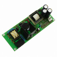
EVAL BOARD FOR NCP1271ADAPG
Manufacturer
ON Semiconductor
Datasheets
1.NCP1271P100G.pdf
(21 pages)
2.NCP1271ADAPGEVB.pdf
(1 pages)
3.NCP1271ADAPGEVB.pdf
(10 pages)
Specifications of NCP1271ADAPGEVB
Design Resources
NCP1271 Adapter EVB BOM NCP1271ADAPGEVB Gerber Files NCP1271EVB Schematic
Main Purpose
AC/DC, Primary Side
Outputs And Type
1, Isolated
Voltage - Output
19V
Current - Output
3A
Voltage - Input
85 ~ 265VAC
Regulator Topology
Flyback
Frequency - Switching
65kHz
Board Type
Fully Populated
Utilized Ic / Part
NCP1271
Silicon Manufacturer
On Semiconductor
Silicon Core Number
NCP1271
Kit Application Type
Power Management
Application Sub Type
PWM Controller
Peak Reflow Compatible (260 C)
No
Rohs Compliant
No
Lead Free Status / RoHS Status
Lead free / RoHS Compliant
Power - Output
-
Lead Free Status / Rohs Status
Lead free / RoHS Compliant
Other names
NCP1271ADAPGEVBOS


turn ratio (n1/n2). The Continuous Conduction Mode
(CCM) lossless flyback is with the following basic
conversion equation.
duty ratio.
Rearrange the equation, it gives:
ratio n
low line conditions respectively that are well within the
allowable duty ratio constraint and the worst−case
MOSFET and diode stress are acceptable.
Lower the diode stress V
MOSFET stress V
MOSFET stress here excludes the consideration of the
leakage inductance that will be covered later. The diode
stress is a little bit close to 100 V limitation of MBR3100 but
that is okay since 400 V input voltage will not exist in real
application.
Step 3b. Define the Primary Current Limit
limits the maximum power that the circuit can be
transferred. In flyback topology, the input current is always
discontinuous and it conducts when duty is on. Hence, the
maximum input power with zero current ripple (infinity
inductance) is 200 W at low line 100 V when I
That is the worst case. It is enough for the 57 W
(19 V × 3.0 A) output power and the 200 W will be reduced
when it goes to finite inductance and DCM later.
V diode + V out )
V
With the assumption that the primary−to−secondary turn
It is a trade−off here in picking the appropriate turn ratio.
The primary current limit (or the peak current) I
in
is the input voltage. V
1
/n
V MOSFET + V in )
D high_line +
D low_line +
2
is 5. It gives 20% and 50% duty ratio at high and
D +
n 2
n 1
V out ) V d
+ 400 ) 5 · (19 ) 1) + 500 V
MOSFET
+
+
V in )
V in + 19 ) 1
V in )
V in
400 ) 5 · (19 ) 1)
100 ) 5 · (19 ) 1)
V in )
I
diode
n 1
n 2
pk
n
n 1
n 2
1
n 1
n 2
5 · (19 ) 1)
5 · (19 ) 1)
(V out ) V d )
/n
. It is noted that the reflected
out
= 4.0 A
(V out ) V d )
n 1
n 2
(V out ) V d )
n 1
n 2
2
n 1
n 2
n 1
n 2
always comes with higher the
+
(V out ) V d )
is the output voltage. D is the
= 5
(V out ) V d )
(V out ) V d )
(V out ) V d )
n 2
n 1
5
1−D
· 400 + 99 V
D
+ 20%
+ 50%
pk
pk
= 4.0 A.
directly
(eq. 1)
(eq. 2)
(eq. 3)
(eq. 4)
(eq. 5)
(eq. 6)
http://onsemi.com
AND8242/D
3
Step 3c. Define the Primary Inductance
inductor equation V = L di/dt.
is selected smaller than the above reference.
Step 3d. DCM Parameter Study
duty ratio D of the DCM operation can be obtained by the
V = L di/dt equation again.
calculated.
L high−line, CCM, lossless +
L low−line, CCM, lossless +
The inductance L selection is based on the fundamental
In order to have the circuit operate in DCM, the inductor
Based on the defined inductor L and peak current I
The equation of DCM flyback is:
Based on this equation, the discharge duty D
D high−line +
D low−line +
D 2−high−line +
P
in(max)
Magnetizing current
Figure 3. DCM Magnetizing Current
= D @ V
D
f
+ 4 · 65
+ 4 · 65
I pk fL
I pk fL
V in
+ 400 · 11.7%
V in
in
V out ) V d
(19 ) 1) · 5
D
V out
1
f
@ I
f
V in
L = 180 mH
2
V in
pk
10 3 · 180
10 3 · 180
+
= 50% @ 100 @ 4 = 200 W
+ 400 · 20%
+ 100 · 50%
400
100
V in D
n 2
n 1
I pk f
4 · 65
4 · 65
V in D
I pk f
n 2
n 1
D 2
D
+ 46.8%
@ D
10 3
10 3
10 −6
10 −6
time
+ 307.7 mH
+ 192.31 mH
+ 11.7%
+ 46.8%
(eq. 10)
(eq. 12)
(eq. 11)
(eq. 7)
(eq. 8)
(eq. 9)
pk
2
, the
is
Related parts for NCP1271ADAPGEVB
Image
Part Number
Description
Manufacturer
Datasheet
Request
R

Part Number:
Description:
ON Semiconductor [VOLTAGE REGULATOR]
Manufacturer:
ON Semiconductor
Datasheet:
Part Number:
Description:
357-036-542-201 CARDEDGE 36POS DL .156 BLK LOPRO
Manufacturer:
ON Semiconductor
Datasheet:
Part Number:
Description:
357-036-542-201 CARDEDGE 36POS DL .156 BLK LOPRO
Manufacturer:
ON Semiconductor
Datasheet:
Part Number:
Description:
357-036-542-201 CARDEDGE 36POS DL .156 BLK LOPRO
Manufacturer:
ON Semiconductor
Datasheet:
Part Number:
Description:
357-036-542-201 CARDEDGE 36POS DL .156 BLK LOPRO
Manufacturer:
ON Semiconductor
Datasheet:
Part Number:
Description:
357-036-542-201 CARDEDGE 36POS DL .156 BLK LOPRO
Manufacturer:
ON Semiconductor
Datasheet:
Part Number:
Description:
357-036-542-201 CARDEDGE 36POS DL .156 BLK LOPRO
Manufacturer:
ON Semiconductor
Datasheet:
Part Number:
Description:
357-036-542-201 CARDEDGE 36POS DL .156 BLK LOPRO
Manufacturer:
ON Semiconductor
Datasheet:
Part Number:
Description:
357-036-542-201 CARDEDGE 36POS DL .156 BLK LOPRO
Manufacturer:
ON Semiconductor
Datasheet:
Part Number:
Description:
357-036-542-201 CARDEDGE 36POS DL .156 BLK LOPRO
Manufacturer:
ON Semiconductor
Datasheet:
Part Number:
Description:
357-036-542-201 CARDEDGE 36POS DL .156 BLK LOPRO
Manufacturer:
ON Semiconductor
Datasheet:
Part Number:
Description:
Manufacturer:
ON Semiconductor
Datasheet:
Part Number:
Description:
Manufacturer:
ON Semiconductor
Datasheet:
Part Number:
Description:
Manufacturer:
ON Semiconductor
Datasheet: