NCP1271ADAPGEVB ON Semiconductor, NCP1271ADAPGEVB Datasheet - Page 4
NCP1271ADAPGEVB
Manufacturer Part Number
NCP1271ADAPGEVB
Description
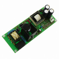
EVAL BOARD FOR NCP1271ADAPG
Manufacturer
ON Semiconductor
Datasheets
1.NCP1271P100G.pdf
(21 pages)
2.NCP1271ADAPGEVB.pdf
(1 pages)
3.NCP1271ADAPGEVB.pdf
(10 pages)
Specifications of NCP1271ADAPGEVB
Design Resources
NCP1271 Adapter EVB BOM NCP1271ADAPGEVB Gerber Files NCP1271EVB Schematic
Main Purpose
AC/DC, Primary Side
Outputs And Type
1, Isolated
Voltage - Output
19V
Current - Output
3A
Voltage - Input
85 ~ 265VAC
Regulator Topology
Flyback
Frequency - Switching
65kHz
Board Type
Fully Populated
Utilized Ic / Part
NCP1271
Silicon Manufacturer
On Semiconductor
Silicon Core Number
NCP1271
Kit Application Type
Power Management
Application Sub Type
PWM Controller
Peak Reflow Compatible (260 C)
No
Rohs Compliant
No
Lead Free Status / RoHS Status
Lead free / RoHS Compliant
Power - Output
-
Lead Free Status / Rohs Status
Lead free / RoHS Compliant
Other names
NCP1271ADAPGEVBOS


< 100%.
in DCM is 93.6 W. That is more than enough (at
57 W/93.6 W = 60.9% efficiency) to deliver the required
output power of 3.0 A × 19 V = 57 W.
Step 3e. Snubber Calculation
voltage stress on the MOSFET because of transformer
leakage inductance. Hence, the calculation starts with the
leakage inductance. From the transformer specification, the
maximum leakage inductance is 2.5 mH. When the leakage
inductance is charged with the peak current 4.0 A, the
maximum possible power to be stored there is 1.3 W.
this 1.3 W, the voltage across this snubber resistor will be
360.6 V.
inductance will be 400 + 360.6 = 760.6 V and it is under the
800 V maximum allowable limit.
307 pF. A 10 nF capacitor is used here.
C snubber w
Step 4. Special Setting on NCP1271 Circuit
the circuit using NCP1271.
P in + 1
Hence, the DCM operation is confirmed here for D + D
In an energy perspective, the total maximum input power
The objective of flyback snubber is to limit the transient
If a 2−Watt 100 kΩ snubber resistor is used to dissipate
Thus, the maximum MOSFET stress due to the leakage
The minimum capacitor to deliver this power will be
This section describes how to set the circuit parameter in
P snubber + 1
D 2−low−line +
P snubber v 1
2
V snubber + P snubber · R snubber
LI 2 f + 1
+ 1
V snubber 2 · f
2 · P snubber
2
2
2
P snubber +
· L leakage · I pk 2 · f
· 2.5
· 180
+ 1.3 · 100
+ 100 · 46.8%
2
· C snubber · V snubber 2 · f
V out ) V d
(19 ) 1) · 5
V in
10 −6 · 4 2 · 65
10 −6 · 4 2 · 65
+
360.6 2 · 65
V snubber 2
R snubber
n 2
n 1
+ 46.8%
10 3 + 360.6 V
@ D
2 · 1.3
10 3 + 1.3 W
10 3 + 93.6 W
10 3
+ 307 pF
(eq. 13)
(eq. 14)
(eq. 15)
(eq. 16)
(eq. 17)
(eq. 18)
(eq. 19)
http://onsemi.com
AND8242/D
2
4
Step 4a. Optional Output OVP Latch
latch circuit. When output voltage is too high, a current from
the optocoupler pulls high the latch pin (Pin 1) voltage and
eventually latches off the controller.
leakage current 50 mA at 22 V. It means that there is an
up−to−50−mA current flowing through the Zener when the
biasing voltage is somewhere below 22 V. This leakage
current can let the optocoupler conducts and triggers the
OVP latch even if the voltage is below the OVP threshold.
In order to prevent it, a R13 resistor is added to bypass the
leakage current. The typical optocoupler diode forward
voltage drop is 1.25 V and the value of R13 is 1.25 V ÷
50 mA = 25 W. Hence, the OVP threshold includes the Zener
biasing voltage 22 V (with "5% tolerance) and the
optocoupler input diode forward bias voltage (1.25 V
typical). As long as it is lower than the 25 V rating of the
output capacitor, it’s fine.
default 1.0 V skip level, the Pin 1 voltage is tied to the
internal bias voltage of the NCP1271. That is typically 6.5 V.
When a R5 34.8 kW skip resistor is used, the nominal Pin 1
voltage goes down to 34.8 kW × 43 mA = 1.5 V. Hence, it is
always recommended to put a skip resistor on Pin 1 to make
sure that there is a good margin between the 8.0 V latch
threshold and the nominal Pin 1 voltage to prevent fault
triggering due to noise or leakage current from the latch
protection circuit.
the latch protection pin to increase noise immunity there. In
order to pull the Pin 1 voltage above the 8.0 V (typical) latch
threshold, a greater−than−8.0−V source is needed. That is
D9
1N5358B
(22V @ 50mA)
Figure 4 shows the output overvoltage protection (OVP)
In implementation, the Zener diode, D9 1N5358B, has a
The latch threshold is 8.0 V. When Pin 1 is opened for
In addition, an nF−order capacitor is generally added to
R13
Figure 4. Output Overvoltage Protection Scheme
25
V out
34.8k 1.2 nF
R5
opto
coupler
C4
R3 200
1
2
3
4
NCP1271
8
6
5
D10
MZP4746
(18 V)
Related parts for NCP1271ADAPGEVB
Image
Part Number
Description
Manufacturer
Datasheet
Request
R

Part Number:
Description:
ON Semiconductor [VOLTAGE REGULATOR]
Manufacturer:
ON Semiconductor
Datasheet:
Part Number:
Description:
357-036-542-201 CARDEDGE 36POS DL .156 BLK LOPRO
Manufacturer:
ON Semiconductor
Datasheet:
Part Number:
Description:
357-036-542-201 CARDEDGE 36POS DL .156 BLK LOPRO
Manufacturer:
ON Semiconductor
Datasheet:
Part Number:
Description:
357-036-542-201 CARDEDGE 36POS DL .156 BLK LOPRO
Manufacturer:
ON Semiconductor
Datasheet:
Part Number:
Description:
357-036-542-201 CARDEDGE 36POS DL .156 BLK LOPRO
Manufacturer:
ON Semiconductor
Datasheet:
Part Number:
Description:
357-036-542-201 CARDEDGE 36POS DL .156 BLK LOPRO
Manufacturer:
ON Semiconductor
Datasheet:
Part Number:
Description:
357-036-542-201 CARDEDGE 36POS DL .156 BLK LOPRO
Manufacturer:
ON Semiconductor
Datasheet:
Part Number:
Description:
357-036-542-201 CARDEDGE 36POS DL .156 BLK LOPRO
Manufacturer:
ON Semiconductor
Datasheet:
Part Number:
Description:
357-036-542-201 CARDEDGE 36POS DL .156 BLK LOPRO
Manufacturer:
ON Semiconductor
Datasheet:
Part Number:
Description:
357-036-542-201 CARDEDGE 36POS DL .156 BLK LOPRO
Manufacturer:
ON Semiconductor
Datasheet:
Part Number:
Description:
357-036-542-201 CARDEDGE 36POS DL .156 BLK LOPRO
Manufacturer:
ON Semiconductor
Datasheet:
Part Number:
Description:
Manufacturer:
ON Semiconductor
Datasheet:
Part Number:
Description:
Manufacturer:
ON Semiconductor
Datasheet:
Part Number:
Description:
Manufacturer:
ON Semiconductor
Datasheet: