NCP3163INVEVB ON Semiconductor, NCP3163INVEVB Datasheet - Page 10
NCP3163INVEVB
Manufacturer Part Number
NCP3163INVEVB
Description
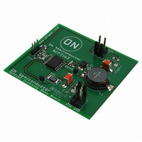
EVAL BOARD FOR NCP3163INV
Manufacturer
ON Semiconductor
Datasheet
1.NCP3163BMNR2G.pdf
(20 pages)
Specifications of NCP3163INVEVB
Design Resources
NCP3163 Inverting EVB BOM NCP3163INVEVB Gerber Files NCP3163 Voltage Inverting EVB Schematic
Main Purpose
DC/DC, Negative Inverter
Outputs And Type
1, Non-Isolated
Voltage - Output
-15V
Current - Output
500mA
Voltage - Input
12V
Regulator Topology
Inverting
Frequency - Switching
150kHz
Board Type
Fully Populated
Utilized Ic / Part
NCP3163
Lead Free Status / RoHS Status
Lead free / RoHS Compliant
Power - Output
-
Lead Free Status / Rohs Status
Lead free / RoHS Compliant
For Use With/related Products
NCP3163INV
Other names
NCP3163INVEVBOS


applications (see application notes at the end of this
document) the inductor will forward bias the output rectifier
when the switch turns off. Rectifiers with a high forward
voltage drop or long turn−on delay time should not be used.
If the emitter is allowed to go sufficiently negative, collector
current will flow, causing additional device heating and
reduced conversion efficiency.
collector current will be in the range 10 mA over
temperature. A 1N5822 or equivalent Schottky barrier
rectifier is recommended to fulfill these requirements.
saturation voltage in step−down and voltage−inverting
converter applications. This input is connected through a
series resistor and capacitor to the switch emitter and is used
to raise the internal 2.0 mA bias current source above V
An internal zener limits the bootstrap input voltage to V
+7.0 V. The capacitor’s equivalent series resistance must
limit the zener current to less than 100 mA. An additional
series resistor may be required when using tantalum or other
of the NCP3163. Three main converter topologies are
demonstrated with actual test data shown below each of the
circuit diagrams. Figure 22 gives the relevant design
When configured for step−down or voltage−inverting
Figure 12 shows that by clamping the emitter to 0.5 V, the
A bootstrap input is provided to reduce the output switch
Figures 23 through 30 show the simplicity and flexibility
Vias to 2nd Layer Metal
for Maximum Heat Sinking
Figure 21. Layout Guidelines to Obtain Maximum
Flare Metal for Maximum Heat Sinking
Package Power Dissipation
http://onsemi.com
0.175
APPLICATIONS
CC
CC
.
0.145
10
low ESR capacitors. The equation below is used to calculate
a minimum value bootstrap capacitor based on a minimum
zener voltage and an upper limit current source.
a supply voltage range of 2.5 V to 40 V. When operating
below 3.0 V, the Bootstrap Input should be connected to
V
1.7 V at room temperature is possible.
Package
plastic package in which the die is mounted on a special heat
tab copper alloy pad. This pad is designed to be soldered
directly to a GND connection on the printed circuit board to
improve thermal conduction. Since this pad directly
contacts the substrate of the die, it is important that this pad
be always soldered to GND, even if surface mount heat
sinking is not being used. Figure 21 shows recommended
layout techniques for this package.
equations for the key parameters. Additionally, a complete
application design aid for the NCP3163 can be found at
www.onsemi.com.
CC
Parametric operation of the NCP3163 is guaranteed over
The NCP3163 is contained in a heatsinkable 16−lead
. Figure 18 shows that functional operation down to
C B(min) + I Dt
0.188
Exposed Pad
DV
Minimum
Recommended
Exposed Copper
+ 4.0 mA
4.0 V
t on
+ 0.001 t on
Related parts for NCP3163INVEVB
Image
Part Number
Description
Manufacturer
Datasheet
Request
R

Part Number:
Description:
3.4 A, Stepup/down/inverting 50300 Khz Switching Regulator
Manufacturer:
ON Semiconductor
Datasheet:

Part Number:
Description:
EVAL BOARD FOR NCP3163BST
Manufacturer:
ON Semiconductor
Datasheet:
Part Number:
Description:
ON Semiconductor [VOLTAGE REGULATOR]
Manufacturer:
ON Semiconductor
Datasheet:
Part Number:
Description:
357-036-542-201 CARDEDGE 36POS DL .156 BLK LOPRO
Manufacturer:
ON Semiconductor
Datasheet:
Part Number:
Description:
357-036-542-201 CARDEDGE 36POS DL .156 BLK LOPRO
Manufacturer:
ON Semiconductor
Datasheet:
Part Number:
Description:
357-036-542-201 CARDEDGE 36POS DL .156 BLK LOPRO
Manufacturer:
ON Semiconductor
Datasheet:
Part Number:
Description:
357-036-542-201 CARDEDGE 36POS DL .156 BLK LOPRO
Manufacturer:
ON Semiconductor
Datasheet:
Part Number:
Description:
357-036-542-201 CARDEDGE 36POS DL .156 BLK LOPRO
Manufacturer:
ON Semiconductor
Datasheet:
Part Number:
Description:
357-036-542-201 CARDEDGE 36POS DL .156 BLK LOPRO
Manufacturer:
ON Semiconductor
Datasheet:
Part Number:
Description:
357-036-542-201 CARDEDGE 36POS DL .156 BLK LOPRO
Manufacturer:
ON Semiconductor
Datasheet:
Part Number:
Description:
357-036-542-201 CARDEDGE 36POS DL .156 BLK LOPRO
Manufacturer:
ON Semiconductor
Datasheet:
Part Number:
Description:
357-036-542-201 CARDEDGE 36POS DL .156 BLK LOPRO
Manufacturer:
ON Semiconductor
Datasheet:
Part Number:
Description:
357-036-542-201 CARDEDGE 36POS DL .156 BLK LOPRO
Manufacturer:
ON Semiconductor
Datasheet:
Part Number:
Description:
Manufacturer:
ON Semiconductor
Datasheet: