NCP3163INVEVB ON Semiconductor, NCP3163INVEVB Datasheet - Page 9
NCP3163INVEVB
Manufacturer Part Number
NCP3163INVEVB
Description
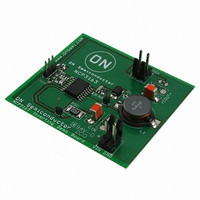
EVAL BOARD FOR NCP3163INV
Manufacturer
ON Semiconductor
Datasheet
1.NCP3163BMNR2G.pdf
(20 pages)
Specifications of NCP3163INVEVB
Design Resources
NCP3163 Inverting EVB BOM NCP3163INVEVB Gerber Files NCP3163 Voltage Inverting EVB Schematic
Main Purpose
DC/DC, Negative Inverter
Outputs And Type
1, Non-Isolated
Voltage - Output
-15V
Current - Output
500mA
Voltage - Input
12V
Regulator Topology
Inverting
Frequency - Switching
150kHz
Board Type
Fully Populated
Utilized Ic / Part
NCP3163
Lead Free Status / RoHS Status
Lead free / RoHS Compliant
Power - Output
-
Lead Free Status / Rohs Status
Lead free / RoHS Compliant
For Use With/related Products
NCP3163INV
Other names
NCP3163INVEVBOS


Feedback and Low Voltage Indicator Comparators
comparator. The inverting input is internally biased at 1.25 V
and is not pinned out. The converter output voltage is
typically divided down with two external resistors and
monitored by the high impedance noninverting input at Pin 2.
The maximum input bias current is ±0.4 mA, which can cause
an output voltage error that is equal to the product of the input
bias current and the upper divider resistance value. For
applications that require 5.0 V, the converter output can be
directly connected to the noninverting input at Pin 3. The high
impedance input, Pin 2, must be grounded to prevent noise
pickup. The internal resistor divider is set for a nominal
voltage of 5.05 V. The additional 50 mV compensates for a
1.0% voltage drop in the cable and connector from the
converter output to the load. The Feedback comparator’s
Current Limit Comparator, Latch and Thermal
Shutdown
normal conditions, output switch conduction is initiated by
the oscillator and terminated by the Voltage Feedback
comparator. Abnormal operating conditions occur when the
converter output is overloaded or when feedback voltage
sensing is lost. Under these conditions, the Current Limit
comparator will protect the Output Switch.
a fractional ohm resistor, R
switch transistor Q
monitored by the Current Sense comparator. If the voltage
drop exceeds 250 mV with respect to V
will set the latch and terminate output switch conduction on
a
configuration ensures that the Output Switch has only a
single on−time during a given oscillator cycle. The
calculation for a value of R
threshold is tightly controlled over temperature and has a
typical input bias current of 1.0 mA. The propagation delay
from the comparator input to the Output Switch is typically
Output voltage control is established by the Feedback
With a voltage mode ripple converter operating under
The switch current is converted to a voltage by inserting
Figures 14 and 15 show that the Current Sense comparator
cycle−by−cycle
R SC +
Indicator Output
2
. The voltage drop across R
Low Voltage
basis.
SC
SC
I pk (Switch)
, in series with V
0.25 V
is:
This
Figure 20. Partial Application Schematic Showing
Implementation of LVI Delay with R
CC
R
C
Comparator/Latch
LVI
DLY
, the comparator
3
2
1
CC
LVI
and output
+
+
-
http://onsemi.com
SC
1.125 V
1.25 V
+
+
-
is
(Bottom View)
9
Feedback
Comparator
output state is controlled by the highest voltage applied to
either of the two noninverting inputs.
for use as a reset controller in microprocessor−based
systems. The inverting input is internally biased at 1.125 V,
which sets the noninverting input thresholds to 90% of
nominal. The LVI comparator has 15 mV of hysteresis to
prevent erratic reset operation. The Open Collector output is
capable of sinking in excess of 6.0 mA (see Figure 13). An
external resistor (R
program a reset delay time (t
below, where V
threshold. Refer to Figure 20.
200 ns. The parasitic inductance associated with R
circuit layout should be minimized. This will prevent
unwanted voltage spikes that may falsely trip the Current
Limit comparator.
the IC in the event that the maximum junction temperature
is exceeded. When activated, typically at 170°C, the Latch
is forced into the “Set” state, disabling the Output Switch.
This feature is provided to prevent catastrophic failures from
accidental device overheating. It is not intended to be used
as a replacement for proper heatsinking.
Driver and Output Switch
efficiency, the driver current source and collector, and
output switch collector and emitter are pinned out
separately. This allows the designer the option of driving the
output switch into saturation with a selected force gain or
driving it near saturation when connected as a Darlington.
The output switch has a typical current gain of 70 at 2.5 A
and is designed to switch a maximum of 40 V collector to
emitter, with up to 3.4 A peak collector current. The
minimum value for R
The Low Voltage Indicator (LVI) comparator is designed
Internal thermal shutdown circuitry is provided to protect
To aid in system design flexibility and conversion
t
DLY
LVI
= R
and C
R SC(min) +
LVI
14
15
16
th(MPU)
⋅ C
DLY
LVI
DLY
SC
) and capacitor (C
L
is the microprocessor reset input
is:
⋅ In
C
0.25 V
3.4 A
O
DLY
1 −
V
+ 0.0735 W
out
) by the formula shown
V
th(MPU)
V
DLY
1
out
) can be used to
SC
and the
Related parts for NCP3163INVEVB
Image
Part Number
Description
Manufacturer
Datasheet
Request
R

Part Number:
Description:
3.4 A, Stepup/down/inverting 50300 Khz Switching Regulator
Manufacturer:
ON Semiconductor
Datasheet:

Part Number:
Description:
EVAL BOARD FOR NCP3163BST
Manufacturer:
ON Semiconductor
Datasheet:
Part Number:
Description:
ON Semiconductor [VOLTAGE REGULATOR]
Manufacturer:
ON Semiconductor
Datasheet:
Part Number:
Description:
357-036-542-201 CARDEDGE 36POS DL .156 BLK LOPRO
Manufacturer:
ON Semiconductor
Datasheet:
Part Number:
Description:
357-036-542-201 CARDEDGE 36POS DL .156 BLK LOPRO
Manufacturer:
ON Semiconductor
Datasheet:
Part Number:
Description:
357-036-542-201 CARDEDGE 36POS DL .156 BLK LOPRO
Manufacturer:
ON Semiconductor
Datasheet:
Part Number:
Description:
357-036-542-201 CARDEDGE 36POS DL .156 BLK LOPRO
Manufacturer:
ON Semiconductor
Datasheet:
Part Number:
Description:
357-036-542-201 CARDEDGE 36POS DL .156 BLK LOPRO
Manufacturer:
ON Semiconductor
Datasheet:
Part Number:
Description:
357-036-542-201 CARDEDGE 36POS DL .156 BLK LOPRO
Manufacturer:
ON Semiconductor
Datasheet:
Part Number:
Description:
357-036-542-201 CARDEDGE 36POS DL .156 BLK LOPRO
Manufacturer:
ON Semiconductor
Datasheet:
Part Number:
Description:
357-036-542-201 CARDEDGE 36POS DL .156 BLK LOPRO
Manufacturer:
ON Semiconductor
Datasheet:
Part Number:
Description:
357-036-542-201 CARDEDGE 36POS DL .156 BLK LOPRO
Manufacturer:
ON Semiconductor
Datasheet:
Part Number:
Description:
357-036-542-201 CARDEDGE 36POS DL .156 BLK LOPRO
Manufacturer:
ON Semiconductor
Datasheet:
Part Number:
Description:
Manufacturer:
ON Semiconductor
Datasheet: