NCP3163INVEVB ON Semiconductor, NCP3163INVEVB Datasheet - Page 2
NCP3163INVEVB
Manufacturer Part Number
NCP3163INVEVB
Description
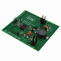
EVAL BOARD FOR NCP3163INV
Manufacturer
ON Semiconductor
Datasheet
1.NCP3163BMNR2G.pdf
(20 pages)
Specifications of NCP3163INVEVB
Design Resources
NCP3163 Inverting EVB BOM NCP3163INVEVB Gerber Files NCP3163 Voltage Inverting EVB Schematic
Main Purpose
DC/DC, Negative Inverter
Outputs And Type
1, Non-Isolated
Voltage - Output
-15V
Current - Output
500mA
Voltage - Input
12V
Regulator Topology
Inverting
Frequency - Switching
150kHz
Board Type
Fully Populated
Utilized Ic / Part
NCP3163
Lead Free Status / RoHS Status
Lead free / RoHS Compliant
Power - Output
-
Lead Free Status / Rohs Status
Lead free / RoHS Compliant
For Use With/related Products
NCP3163INV
Other names
NCP3163INVEVBOS


PIN FUNCTION DESCRIPTION
Exposed
SOIC16
5,12,13
14,15
10,11
Pad
16
1
2
3
4
6
7
8
9
Shutdown
10,11,12,13
Exposed
DFN18
6,7,8,9
Pad
15
16
17
18
14
1
3
4
5
2
Voltage Feedback 1
Voltage Feedback 2
Timing Capacitor
Voltage Feedback 2
Voltage Feedback 1
V
I
LVI Output
PKsense
Timing Capacitor
Switch Collector
CC
Bootstrap Input
Drive Collector
Switch Emitter
R
Exposed Pad
R
No Connect
PIN NAME
LVI Output
C
DT
Gnd
I
SC
pk
T
GND
V
Sense
CC
8
7
6
5
4
3
2
1
Figure 2. Representative Block Diagram
LVI
V
0.25 V
CC
Oscillator
Thermal
+
+
-
This pin will sink current when FB1 and FB2 are less than the LVI threshold (V
Connecting this pin to a resistor divider off of the output will regulate the application
according to the V
Connecting this pin directly to the output will regulate the device to 5.05 V.
Ground pin for all internal circuits and power switch.
Connect a capacitor to this pin to set the frequency. The addition of a parallel resist-
or will decrease the maximum duty cycle and increase the frequency.
Power pin for the IC.
When (V
pulse basis.
Voltage driver collector
Internal switch transistor collector
Internal switch transistor emitter
Connect this pin to V
series resistor and capacitor can be utilized to improve the converter efficiency.
These pins have no connection.
The exposed pad beneath the package must be connected to GND (pin 4). Addi-
tionally, using proper layout techniques, the exposed pad can greatly enhance the
power dissipation capabilities of the NCP3163.
-
+
1.125 V
http://onsemi.com
45 k
Current
1.25 V
+
+
-
Limit
CC
(Bottom View)
−V
Comparator
IPKsense
2
Feedback
15 k
V
2.0 mA
CC
out
Latch
R
S
CC
Q
design equation in Figure 22.
) > 250 mV the circuit resets the output driver on a pulse by
V
for operation at low V
CC
7.0 V
Q1
60
Q2
DESCRIPTION
10
12
13
14
15
16
11
9
Bootstrap Input
Driver Collector
Switch Collector
CC
Switch Emitter
levels. For some topologies, a
+
-
= Sink Only
Positive True Logic
th
).
Related parts for NCP3163INVEVB
Image
Part Number
Description
Manufacturer
Datasheet
Request
R

Part Number:
Description:
3.4 A, Stepup/down/inverting 50300 Khz Switching Regulator
Manufacturer:
ON Semiconductor
Datasheet:

Part Number:
Description:
EVAL BOARD FOR NCP3163BST
Manufacturer:
ON Semiconductor
Datasheet:
Part Number:
Description:
ON Semiconductor [VOLTAGE REGULATOR]
Manufacturer:
ON Semiconductor
Datasheet:
Part Number:
Description:
357-036-542-201 CARDEDGE 36POS DL .156 BLK LOPRO
Manufacturer:
ON Semiconductor
Datasheet:
Part Number:
Description:
357-036-542-201 CARDEDGE 36POS DL .156 BLK LOPRO
Manufacturer:
ON Semiconductor
Datasheet:
Part Number:
Description:
357-036-542-201 CARDEDGE 36POS DL .156 BLK LOPRO
Manufacturer:
ON Semiconductor
Datasheet:
Part Number:
Description:
357-036-542-201 CARDEDGE 36POS DL .156 BLK LOPRO
Manufacturer:
ON Semiconductor
Datasheet:
Part Number:
Description:
357-036-542-201 CARDEDGE 36POS DL .156 BLK LOPRO
Manufacturer:
ON Semiconductor
Datasheet:
Part Number:
Description:
357-036-542-201 CARDEDGE 36POS DL .156 BLK LOPRO
Manufacturer:
ON Semiconductor
Datasheet:
Part Number:
Description:
357-036-542-201 CARDEDGE 36POS DL .156 BLK LOPRO
Manufacturer:
ON Semiconductor
Datasheet:
Part Number:
Description:
357-036-542-201 CARDEDGE 36POS DL .156 BLK LOPRO
Manufacturer:
ON Semiconductor
Datasheet:
Part Number:
Description:
357-036-542-201 CARDEDGE 36POS DL .156 BLK LOPRO
Manufacturer:
ON Semiconductor
Datasheet:
Part Number:
Description:
357-036-542-201 CARDEDGE 36POS DL .156 BLK LOPRO
Manufacturer:
ON Semiconductor
Datasheet:
Part Number:
Description:
Manufacturer:
ON Semiconductor
Datasheet: