NCP3163INVEVB ON Semiconductor, NCP3163INVEVB Datasheet - Page 16
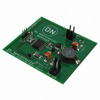
NCP3163INVEVB
Manufacturer Part Number
NCP3163INVEVB
Description
EVAL BOARD FOR NCP3163INV
Manufacturer
ON Semiconductor
Datasheet
1.NCP3163BMNR2G.pdf
(20 pages)
Specifications of NCP3163INVEVB
Design Resources
NCP3163 Inverting EVB BOM NCP3163INVEVB Gerber Files NCP3163 Voltage Inverting EVB Schematic
Main Purpose
DC/DC, Negative Inverter
Outputs And Type
1, Non-Isolated
Voltage - Output
-15V
Current - Output
500mA
Voltage - Input
12V
Regulator Topology
Inverting
Frequency - Switching
150kHz
Board Type
Fully Populated
Utilized Ic / Part
NCP3163
Lead Free Status / RoHS Status
Lead free / RoHS Compliant
Power - Output
-
Lead Free Status / Rohs Status
Lead free / RoHS Compliant
For Use With/related Products
NCP3163INV
Other names
NCP3163INVEVBOS


Value of Components for V
L
D
C
C
C
in
out
t
Name
Test Results for V
Line Regulation
Load Regulation
Output Ripple
Efficiency
Short Circuit Current
2 A, 40 V Schottky Rectifier
R
T
out
Test
2 X 270 mF, 16 V
V
Figure 29. Typical Voltage Inverting Application Schematic
150 pF ±10%
in
270 mF, 16 V
= −15 V
47 mH
Value
R
out
C
C
SC
R
T
in
2
= −15 V
+
R
1
8
7
6
5
4
3
2
1
V
LVI
CC
0.25 V
Oscillator
V
V
V
V
V
+
+
-
in
in
in
in
in
Thermal
= 12 V, I
= 12 V, R
= 7.0 V to 16 V, I
= 12 V, I
= 12 V, I
http://onsemi.com
45 k
-
+
1.125 V
1.25 V
+
+
-
Current
Limit
(Bottom View)
Condition
out
out
out
L
16
Feedback
Comparator
15 k
= 0.1 W
V
= 500 mA
= 0 to 500 mA
= 0 to 500 mA
CC
Latch
R
R
R
C
R
out
R
S
Q
1
2
sc
b
b
V
CC
= 500 mA
Name
7.0 V
Q
2.0 mA
60
1
Q
2
10
12
13
14
15
16
11
9
R
C
D
B
B
L
Results
100 mVpp
35 mV
20 mV
+
3.1 A
68%
C
O
80 mW, 1 W
1.07 kW
11.8 kW
4.7 nF
200 W
Value
V
out
Related parts for NCP3163INVEVB
Image
Part Number
Description
Manufacturer
Datasheet
Request
R

Part Number:
Description:
3.4 A, Stepup/down/inverting 50300 Khz Switching Regulator
Manufacturer:
ON Semiconductor
Datasheet:

Part Number:
Description:
EVAL BOARD FOR NCP3163BST
Manufacturer:
ON Semiconductor
Datasheet:
Part Number:
Description:
ON Semiconductor [VOLTAGE REGULATOR]
Manufacturer:
ON Semiconductor
Datasheet:
Part Number:
Description:
357-036-542-201 CARDEDGE 36POS DL .156 BLK LOPRO
Manufacturer:
ON Semiconductor
Datasheet:
Part Number:
Description:
357-036-542-201 CARDEDGE 36POS DL .156 BLK LOPRO
Manufacturer:
ON Semiconductor
Datasheet:
Part Number:
Description:
357-036-542-201 CARDEDGE 36POS DL .156 BLK LOPRO
Manufacturer:
ON Semiconductor
Datasheet:
Part Number:
Description:
357-036-542-201 CARDEDGE 36POS DL .156 BLK LOPRO
Manufacturer:
ON Semiconductor
Datasheet:
Part Number:
Description:
357-036-542-201 CARDEDGE 36POS DL .156 BLK LOPRO
Manufacturer:
ON Semiconductor
Datasheet:
Part Number:
Description:
357-036-542-201 CARDEDGE 36POS DL .156 BLK LOPRO
Manufacturer:
ON Semiconductor
Datasheet:
Part Number:
Description:
357-036-542-201 CARDEDGE 36POS DL .156 BLK LOPRO
Manufacturer:
ON Semiconductor
Datasheet:
Part Number:
Description:
357-036-542-201 CARDEDGE 36POS DL .156 BLK LOPRO
Manufacturer:
ON Semiconductor
Datasheet:
Part Number:
Description:
357-036-542-201 CARDEDGE 36POS DL .156 BLK LOPRO
Manufacturer:
ON Semiconductor
Datasheet:
Part Number:
Description:
357-036-542-201 CARDEDGE 36POS DL .156 BLK LOPRO
Manufacturer:
ON Semiconductor
Datasheet:
Part Number:
Description:
Manufacturer:
ON Semiconductor
Datasheet: