EVAL5985 STMicroelectronics, EVAL5985 Datasheet - Page 27
EVAL5985
Manufacturer Part Number
EVAL5985
Description
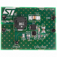
BOARD EVAL FOR L5985
Manufacturer
STMicroelectronics
Type
DC/DC Switching Converters, Regulators & Controllersr
Specifications of EVAL5985
Main Purpose
DC/DC, Step Down
Outputs And Type
1, Non-Isolated
Voltage - Output
3.3V
Current - Output
2A
Voltage - Input
3.3 ~ 18V
Regulator Topology
Buck
Frequency - Switching
500kHz
Board Type
Fully Populated
Utilized Ic / Part
L5985
Input Voltage
2.9 V to 18 V
Output Voltage
0.6 V to 16 V
Product
Power Management Modules
Silicon Manufacturer
ST Micro
Silicon Core Number
L5985
Kit Application Type
Power Management - Voltage Regulator
Application Sub Type
Step Down Switching Regulator
Kit Contents
Board
Lead Free Status / RoHS Status
Lead free / RoHS Compliant
Power - Output
-
Lead Free Status / Rohs Status
Lead free / RoHS Compliant
For Use With/related Products
L5985
Other names
497-6387
EVAL5985
EVAL5985
Available stocks
Company
Part Number
Manufacturer
Quantity
Price


L5985
5.6
Figure 16. Switching losses
Layout considerations
The PC board layout of switching DC/DC regulator is very important to minimize the noise
injected in high impedance nodes and interferences generated by the high switching current
loops.
In a step-down converter the input loop (including the input capacitor, the power MOSFET
and the free wheeling diode) is the most critical one. This is due to the fact that the high
value pulsed current are flowing through it. In order to minimize the EMI, this loop has to be
as short as possible.
The feedback pin (FB) connection to external resistor divider is a high impedance node, so
the interferences can be minimized placing the routing of feedback node as far as possible
from the high current paths. To reduce the pick up noise the resistor divider has to be placed
very close to the device. To filter the high frequency noise, a small capacitor (100 nF) can be
added as close as possible to the input voltage pin of the device.
Thanks to the exposed pad of the device, the ground plane helps to reduce the thermal
resistance junction to ambient; so a large ground plane enhances the thermal performance
of the converter allowing high power conversion.
In
Figure 17
a layout example is shown.
Doc ID 13006 Rev 5
Application information
27/37
Related parts for EVAL5985
Image
Part Number
Description
Manufacturer
Datasheet
Request
R

Part Number:
Description:
STMicroelectronics [RIPPLE-CARRY BINARY COUNTER/DIVIDERS]
Manufacturer:
STMicroelectronics
Datasheet:
Part Number:
Description:
STMicroelectronics [LIQUID-CRYSTAL DISPLAY DRIVERS]
Manufacturer:
STMicroelectronics
Datasheet:

Part Number:
Description:
BOARD EVAL FOR MEMS SENSORS
Manufacturer:
STMicroelectronics
Datasheet:
Part Number:
Description:
NPN TRANSISTOR POWER MODULE
Manufacturer:
STMicroelectronics
Datasheet:
Part Number:
Description:
TURBOSWITCH ULTRA-FAST HIGH VOLTAGE DIODE
Manufacturer:
STMicroelectronics
Datasheet:
Part Number:
Description:
Manufacturer:
STMicroelectronics
Datasheet:
Part Number:
Description:
DIODE / SCR MODULE
Manufacturer:
STMicroelectronics
Datasheet:
Part Number:
Description:
DIODE / SCR MODULE
Manufacturer:
STMicroelectronics
Datasheet:
Part Number:
Description:
Search -----> STE16N100
Manufacturer:
STMicroelectronics
Datasheet:
Part Number:
Description:
Search ---> STE53NA50
Manufacturer:
STMicroelectronics
Datasheet:
Part Number:
Description:
NPN Transistor Power Module
Manufacturer:
STMicroelectronics
Datasheet:
Part Number:
Description:
DIODE / SCR MODULE
Manufacturer:
STMicroelectronics
Datasheet: