STEVAL-ISA022V1 STMicroelectronics, STEVAL-ISA022V1 Datasheet - Page 9
STEVAL-ISA022V1
Manufacturer Part Number
STEVAL-ISA022V1
Description
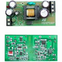
EVAL BOARD 6W POWER SUPPLY
Manufacturer
STMicroelectronics
Series
VIPER™r
Datasheets
1.VIPER12ADIP-E.pdf
(21 pages)
2.VIPER12AS.pdf
(15 pages)
3.STEVAL-ISA022V1.pdf
(4 pages)
Specifications of STEVAL-ISA022V1
Design Resources
STEVAL-ISA022V1 Schematics STEVAL-ISA022V1 Bill of Material
Main Purpose
AC/DC, Primary Side
Outputs And Type
2, Isolated
Power - Output
5.5W
Voltage - Output
5V, 15V
Current - Output
500mA, 200mA
Voltage - Input
90 ~ 264VAC
Regulator Topology
Flyback
Frequency - Switching
60kHz
Board Type
Fully Populated
Utilized Ic / Part
VIPer12A
Product
Power Management Modules
Lead Free Status / RoHS Status
Lead free / RoHS Compliant
Other names
497-5520
Available stocks
Company
Part Number
Manufacturer
Quantity
Price
Company:

Part Number:
STEVAL-ISA022V1
Manufacturer:
STMicroelectronics
Quantity:
135


Figure 9 : Internal Current Control Structure
FEEDBACK PIN PRINCIPLE OF OPERATION
A feedback pin controls the operation of the
device. Unlike conventional PWM control circuits
which use a voltage input (the inverted input of an
operational amplifier), the FB pin is sensitive to
current. Figure 9 presents the internal current
mode structure.
The Power MOSFET delivers a sense current I
which is proportional to the main current Id. R2
receives this current and the current coming from
the FB pin. The voltage across R2 is then
compared to a fixed reference voltage of about
0.23 V. The MOSFET is switched off when the
following equation is reached:
By extracting I
Using the current sense ratio of the MOSFET G
The current limitation is obtained with the FB pin
shorted to ground (V
negative current sourced by this pin, and
expressed by:
I
By reporting this expression in the previous one, it
is possible to obtain the drain current limitation
I
I
I
I
R
Dlim
FB
Dlim
S
D
2
Secondary
feedback
=
=
:
=
I
0.23V
------------- - I
G
=
S
–
R
+
ID
0.23V
------------- -
G
2
R
I
ID
FB
1
I
–
S
S
+Vdd
:
0.23V
FB
=
=
I
C
FB
G
0.23V
ID
FB
FB
----- -
R
= 0 V). This leads to a
1
0.23V
------------- - I
2
R
0.23V
+
1 k
2
R1
----- -
R
230
OSCILLATOR
1
LATCH
1
PWM
60kHz
–
S
R
R2
Q
FB
Is
SOURCE
DRAIN
Id
ID
:
s
In a real application, the FB pin is driven with an
optocoupler as shown on figure 9 which acts as a
pull up. So, it is not possible to really short this pin
to ground and the above drain current value is not
achievable. Nevertheless, the capacitor C is
averaging the voltage on the FB pin, and when the
optocoupler is off (start up or short circuit), it can be
assumed that the corresponding voltage is very
close to 0 V.
For low drain currents, the formula (1) is valid as
long as IFB satisfies I
internal threshold of the VIPer12A. If I
this threshold the device will stop switching. This is
represented on figure 4, and I
specified in the PWM COMPARATOR SECTION.
Actually, as soon as the drain current is about 12%
of Idlim, that is to say 50 mA, the device will enter
a burst mode operation by missing switching
cycles. This is especially important when the
converter is lightly loaded.
It is then possible to build the total DC transfer
function between I
This figure also takes into account the internal
blanking time and its associated minimum turn on
time. This imposes a minimum drain current under
which the device is no more able to control it in a
linear way. This drain current depends on the
primary inductance value of the transformer and
the input voltage. Two cases may occur,
depending on the value of this current versus the
fixed 50 mA value, as described above.
START UP SEQUENCE
This device includes a high voltage start up current
source connected on the drain of the device. As
soon as a voltage is applied on the input of the
converter, this start up current source is activated
as long as V
reaching V
switched off and the device begins to operate by
turning on and off its main power MOSFET. As the
FB pin does not receive any current from the
optocoupler, the device operates at full current
capacity and the output voltage rises until reaching
Figure 10 : I
t
-------------------------------------- -
t
-------------------------------------- -
ONmin
ONmin
L
L
50mA
V
V
I
1
2
Dpeak
IN
IN
0
DDon
FB
I
Dlim
DD
Transfer function
, the start up current source is
D
is lower than V
VIPer12ADIP / VIPer12AS
and I
FB
< I
FB
FBsd
I
as shown on figure 10.
FBsd
Part masked by the
, where I
I
FBsd
FBsd
threshold
DDon
FB
FBsd
value is
exceeds
I
. When
FB
is an
9/15
Related parts for STEVAL-ISA022V1
Image
Part Number
Description
Manufacturer
Datasheet
Request
R

Part Number:
Description:
BOARD RGB CTR ST7,STP08C596MTR
Manufacturer:
STMicroelectronics
Datasheet:

Part Number:
Description:
Power Management IC Development Tools Full Speed USB to RS232 Bridge Demo
Manufacturer:
STMicroelectronics
Datasheet:
Part Number:
Description:
Power Management IC Development Tools 2.5W solar eval BRD USB SPV1040 LD39050
Manufacturer:
STMicroelectronics
Datasheet:

Part Number:
Description:
BOARD EVAL FOR MEMS SENSORS
Manufacturer:
STMicroelectronics
Datasheet:

Part Number:
Description:
KIT DEV STARTER ST10F276Z5
Manufacturer:
STMicroelectronics
Datasheet:

Part Number:
Description:
BOARD EVAL HDMI $ VIDEO SWITCH
Manufacturer:
STMicroelectronics
Datasheet:

Part Number:
Description:
BOARD DEMO ACCELEROMETER DIL24
Manufacturer:
STMicroelectronics
Datasheet:

Part Number:
Description:
BOARD STLM75/STDS75/ST72F651
Manufacturer:
STMicroelectronics
Datasheet:

Part Number:
Description:
EVAL BOARD 3AXIS MEMS ACCELLRMTR
Manufacturer:
STMicroelectronics
Datasheet:

Part Number:
Description:
BOARD EVAL 8BIT MICRO + TDE1708
Manufacturer:
STMicroelectronics
Datasheet:
Part Number:
Description:
STMicroelectronics [RIPPLE-CARRY BINARY COUNTER/DIVIDERS]
Manufacturer:
STMicroelectronics
Datasheet:
Part Number:
Description:
STMicroelectronics [LIQUID-CRYSTAL DISPLAY DRIVERS]
Manufacturer:
STMicroelectronics
Datasheet:
Part Number:
Description:
BOARD EVAL FOR MEMS SENSORS
Manufacturer:
STMicroelectronics
Datasheet: