STEVAL-ISA016V1 STMicroelectronics, STEVAL-ISA016V1 Datasheet
STEVAL-ISA016V1
Specifications of STEVAL-ISA016V1
STEVAL-ISA016V1
Available stocks


Related parts for STEVAL-ISA016V1


STEVAL-ISA016V1 Summary of contents
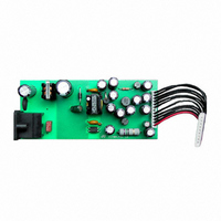
Page 1
QUASI-RESONANT (QR) ZERO-VOLTAGE- SWITCHING (ZVS) TOPOLOGY LINE FEED FORWARD TO DELIVER CONSTANT POWER vs. MAINS CHANGE FREQUENCY FOLDBACK FOR OPTIMUM STANDBY EFFICIENCY PULSE-BY-PULSE & HICCUP-MODE OCP ULTRA-LOW START-UP (< 70µA) AND QUIESCENT CURRENT (< 3.5mA) DISABLE FUNCTION (ON/OFF CONTROL) 1% ...
Page 2
L6565 DESCRIPTION (continued) Converter's power capability variations with the mains voltage are compensated by line voltage feedforward. At light load the device features a special function that automatically lowers the operating frequency still main- taining the operation as close to ...
Page 3
THERMAL DATA Symbol R Max. Thermal Resistance, Junction-to-ambient th j-amb ABSOLUTE MAXIMUM RATINGS Symbol Pin Vcc Output Totem Pole Peak Current (2 µs) GD INV, COMP Analog Inputs ...
Page 4
L6565 ELECTRICAL CHARACTERISTCS (continued -25 to 125° 12V Symbol Parameter G Voltage Gain V GB Gain-Bandwidth Product I Source Current COMP Sink Current V Upper Clamp Voltage COMP Lower Clamp Voltage CURRENT SENSE ...
Page 5
Figure 1. Supply current vs. Supply voltage I CC (mA 0.5 0.1 0.05 0.01 0.005 Figure 2. Start-up & UVLO vs. Temperature 14 V CC-ON ( CC-OFF ...
Page 6
L6565 Figure 7. Gate-drive output saturation V [V] pin7 2 °C Vcc = 14.5 V SINK 2 1 100 200 300 I [mA] GD Figure 8. Gate-drive output saturation V [V] pin7 0 ...
Page 7
APPLICATION INFORMATION Quasi-resonant operation in offline flyback converters lies in synchronizing MOSFET's turn-on to the transform- er's demagnetization. Detecting the resulting negative-going edge of the voltage across any winding of the transformer can do this. The L6565 is provided with ...
Page 8
L6565 Zero Current Detection and Triggering Block (see fig. 13): The Zero Current Detection (ZCD) block switches on the external MOSFET if a negative-going edge falling be- low 1 applied to the input (pin 5, ZCD). However, to ...
Page 9
L6565 puts a limit on the minimum OFF-time of the switch. This is done by blanking the triggering block of the ZCD circuit as mentioned before. The duration of the blanking time (3.5µs min function of the ...
Page 10
L6565 It acts on the clamp level of the control voltage V of the converter's input voltage sensed through a dedicated pin (#3, VFF): the higher the input voltage, the lower the setpoint. This is illustrated in the diagram of ...
Page 11
Error Amplifier Block (see fig. 17b): The Error Amplifier (E/A) inverting input is used in primary feedback technique to compare a partition of the volt- age generated by the auxiliary winding with the internal reference, to achieve converter's output voltage ...
Page 12
L6565 TYPICAL APPLICATIONS Figure 19. 50W Wide Range Mains SMPS for 14" NTC1 16R 2A fuse C25 Vin 1nF C23 C24 88 to 100nF 100nF 264 Vac L1 15mH C26 1nF R3 IC1 3 M L6565 VFF 3 ...
Page 13
APPLICATION IDEAS Here follows a series of ideas/suggestions aimed at either improving performance or solving common applica- tion issues of L6565-based power supplies. Figure 21. Enhanced turn-off for big MOSFET's drive Figure 22. Latched shutdown on: a) feedback disconnection; b) ...
Page 14
L6565 Figure 24. Primary Feedback loop configurations COMP INV R L 2.5V GND 6 a) Figure 25. Protection against secondary feedback disconnection by primary regulation take-over 15 V INV 2.2 k Figure 26. Leading edge blanking ...
Page 15
DIM. MIN. TYP. MAX. MIN. A 3.32 a1 0.51 0.020 B 1.15 1.65 0.045 b 0.356 0.55 0.014 b1 0.204 0.304 0.008 D 10.92 E 7.95 9.75 0.313 e 2.54 e3 7.62 e4 7.62 F 6.6 I 5.08 L ...
Page 16
L6565 mm DIM. MIN. TYP. MAX. A 1.75 a1 0.1 0.25 0.004 a2 1.65 a3 0.65 0.85 0.026 b 0.35 0.48 0.014 b1 0.19 0.25 0.007 C 0.25 0.5 0.010 c1 45 (typ.) D (1) 4.8 5.0 0.189 E 5.8 ...
Page 17
... No license is granted by implication or otherwise under any patent or patent rights of STMicroelectronics. Specifications mentioned in this publication are subject to change without notice. This publication supersedes and replaces all information previously supplied. STMicroelectronics products are not authorized for use as critical components in life support devices or systems without express written approval of STMicroelectronics ...