STEVAL-ISA016V1 STMicroelectronics, STEVAL-ISA016V1 Datasheet - Page 2
STEVAL-ISA016V1
Manufacturer Part Number
STEVAL-ISA016V1
Description
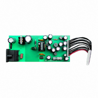
BOARD EVAL L6565 EU220V BASED
Manufacturer
STMicroelectronics
Type
AC/DC Switching Convertersr
Specifications of STEVAL-ISA016V1
Mfg Application Notes
Quasi AppNote
Design Resources
STEVAL-ISA016V1 Gerber Files STEVAL-ISA016V1 Schematic STEVAL-ISA016V1 Bill of Materials
Main Purpose
AC/DC, Primary Side
Outputs And Type
6, Non-Isolated
Power - Output
17W
Voltage - Output
1.23V, 5V, 2.5V, 12V, 3.3V, 8V
Current - Output
1.7A, 1A, 700mA, 500mA, 450mA, 40mA
Voltage - Input
185 ~ 265VAC
Regulator Topology
Flyback
Board Type
Fully Populated
Utilized Ic / Part
L6565
Input Voltage
185 V to 265 V
Output Voltage
1.2 V to 12 V
Product
Power Management Modules
Lead Free Status / RoHS Status
Lead free / RoHS Compliant
Frequency - Switching
-
Lead Free Status / Rohs Status
Lead free / RoHS Compliant
For Use With/related Products
L6565
Other names
497-6414
STEVAL-ISA016V1
STEVAL-ISA016V1
Available stocks
Company
Part Number
Manufacturer
Quantity
Price


L6565
DESCRIPTION (continued)
Converter's power capability variations with the mains voltage are compensated by line voltage feedforward.
At light load the device features a special function that automatically lowers the operating frequency still main-
taining the operation as close to ZVS as possible. In addition to very low start-up and quiescent currents, this
feature helps keep low the consumption from the mains at light load and be Blue Angel and Energy Star com-
pliant.
The IC includes also a disable function, an on-chip filter on current sense, an error amplifier with a precise ref-
erence voltage for primary regulation and an effective two-level overcurrent protection.
PIN CONNECTION (Top view, Minidip and SO8)
PIN DESCRIPTION
2/17
N°
1
2
3
4
5
6
7
8
COMP
Name
GND
ZCD
VFF
INV
Vcc
GD
CS
Inverting input of the error amplifier. The information on the output voltage is fed into the pin
through either a resistor divider (primary regulation) or an optocoupler (secondary feedback).
This pin can be grounded in some secondary feedback schemes (see pin 2).
Output of the error amplifier. Typically, a compensation network is placed between this pin and
the INV pin to achieve stability and good dynamic performance of the voltage control loop. With
secondary feedback, the pin can be also driven directly by an optocoupler to control PWM by
modulating the current sunk from the pin (with the INV pin grounded).
Line voltage feedforward. The information on the converter’s input voltage is fed into the pin
through a resistor divider and is used to change the setpoint of the pulse-by-pulse current
limitation (the higher the voltage, the lower the setpoint). If this function is not desired the pin will
be grounded and the current limitation setpoint will be maximum.
Input to the PWM comparator. The primary current is sensed through a resistor, the resulting
voltage is applied to this pin and compared with an internal reference to determine MOSFET’s
turn-off. The internal reference is clamped at a value, which defines the pulse-by-pulse current
limitation setpoint, depending on the voltage at pin VFF. If the signal at the pin CS exceeds 2 V,
the gate driver will be disabled (Hiccup-mode OCP).
Transformer’s demagnetization sensing input for Quasi-Resonant operation. Alternately,
synchronization input for an external signal. A negative-going edge triggers MOSFET’s turn-on.
The trigger circuit is blanked for a minimum of 3.5 µs after MOSFET turn-off, for safe operation
under short circuit conditions and frequency foldback. If the pin is grounded the IC will be
disabled.
Ground. Current return for both the signal part of the IC and the gate driver.
Gate driver output. The totem pole output stage is able to drive power MOSFET’s and IGBT’s
with a peak current of 400 mA (source and sink).
Supply Voltage of both the signal part of the IC and the gate driver. An electrolytic capacitor is
connected between this pin and ground. A resistor connected from this pin to the converter’s
input bulk capacitor will be typically used to start up the device.
COMP
VFF
INV
CS
1
2
3
4
Function
8
7
6
5
GND
Vcc
GD
ZCD
Related parts for STEVAL-ISA016V1
Image
Part Number
Description
Manufacturer
Datasheet
Request
R

Part Number:
Description:
BOARD RGB CTR ST7,STP08C596MTR
Manufacturer:
STMicroelectronics
Datasheet:

Part Number:
Description:
Power Management IC Development Tools Full Speed USB to RS232 Bridge Demo
Manufacturer:
STMicroelectronics
Datasheet:
Part Number:
Description:
Power Management IC Development Tools 2.5W solar eval BRD USB SPV1040 LD39050
Manufacturer:
STMicroelectronics
Datasheet:

Part Number:
Description:
BOARD EVAL FOR MEMS SENSORS
Manufacturer:
STMicroelectronics
Datasheet:

Part Number:
Description:
KIT DEV STARTER ST10F276Z5
Manufacturer:
STMicroelectronics
Datasheet:

Part Number:
Description:
BOARD EVAL HDMI $ VIDEO SWITCH
Manufacturer:
STMicroelectronics
Datasheet:

Part Number:
Description:
BOARD DEMO ACCELEROMETER DIL24
Manufacturer:
STMicroelectronics
Datasheet:

Part Number:
Description:
BOARD STLM75/STDS75/ST72F651
Manufacturer:
STMicroelectronics
Datasheet:

Part Number:
Description:
EVAL BOARD 3AXIS MEMS ACCELLRMTR
Manufacturer:
STMicroelectronics
Datasheet:

Part Number:
Description:
BOARD EVAL 8BIT MICRO + TDE1708
Manufacturer:
STMicroelectronics
Datasheet:
Part Number:
Description:
STMicroelectronics [RIPPLE-CARRY BINARY COUNTER/DIVIDERS]
Manufacturer:
STMicroelectronics
Datasheet:
Part Number:
Description:
STMicroelectronics [LIQUID-CRYSTAL DISPLAY DRIVERS]
Manufacturer:
STMicroelectronics
Datasheet:
Part Number:
Description:
BOARD EVAL FOR MEMS SENSORS
Manufacturer:
STMicroelectronics
Datasheet: