STEVAL-ISA038V1 STMicroelectronics, STEVAL-ISA038V1 Datasheet - Page 17
STEVAL-ISA038V1
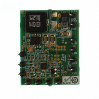
Manufacturer Part Number
STEVAL-ISA038V1
Description
BOARD EVALUATION W/L6728
Manufacturer
STMicroelectronics
Type
DC/DC Switching Converters, Regulators & Controllersr
Specifications of STEVAL-ISA038V1
Design Resources
STEVAL-ISA038V1 Schematic STEVAL-ISA038V1 Bill of Material
Main Purpose
DC/DC, Step Down
Outputs And Type
1, Non-Isolated
Voltage - Output
1.25V
Current - Output
5A
Voltage - Input
5 ~ 12V
Regulator Topology
Buck
Frequency - Switching
300kHz
Board Type
Fully Populated
Utilized Ic / Part
L6728
Input Voltage
5 V to 12 V
Output Voltage
1.25 V
Product
Power Management Modules
Silicon Manufacturer
ST Micro
Silicon Core Number
L6728D
Kit Application Type
Power Management - Voltage Regulator
Application Sub Type
Step Down DC/DC Controller
Kit Contents
Board
Lead Free Status / RoHS Status
Lead free / RoHS Compliant
Power - Output
-
Lead Free Status / Rohs Status
Lead free / RoHS Compliant
For Use With/related Products
L6728
Other names
497-8228
STEVAL-ISA038V1
STEVAL-ISA038V1
Available stocks
Company
Part Number
Manufacturer
Quantity
Price
Company:

Part Number:
STEVAL-ISA038V1
Manufacturer:
STMicroelectronics
Quantity:
1


L6728
10.2
Layout guidelines
L6728 provides control functions and high current integrated drivers to implement high-
current step-down DC-DC converters. In this kind of application, a good layout is very
important.
The first priority when placing components for these applications has to be reserved to the
power section, minimizing the length of each connection and loop as much as possible. To
minimize noise and voltage spikes (EMI and losses) power connections (highlighted in
Figure
traces: loop must be anyway minimized. The critical components, i.e. the power MOSFETs,
must be close one to the other. The use of multi-layer printed circuit board is recommended.
The input capacitance (C
placed close to the power section in order to eliminate the stray inductance generated by the
copper traces. Low ESR and ESL capacitors are preferred, MLCC are suggested to be
connected near the HS drain.
Use proper VIAs number when power traces have to move between different planes on the
PCB in order to reduce both parasitic resistance and inductance. Moreover, reproducing the
same high-current trace on more than one PCB layer will reduce the parasitic resistance
associated to that connection.
Connect output bulk capacitors (C
inductance and resistance associated to the copper trace, also adding extra decoupling
capacitors along the way to the load when this results in being far from the bulk capacitors
bank.
b)
c)
d)
e)
f)
7) must be a part of a power plane and anyway realized by wide and thick copper
Place F
Place F
Place F
Check that compensation network gain is lower than open loop EA gain before
F
Check phase margin obtained (it should be greater than 45°) and repeat if
necessary.
C
R
C
C
0dB
P
S
S
F
=
=
=
=
;
----------------------------------------------------------
2π R
-------------------------- -
------------------------------ -
π R
----------------- - 1
2 F
-----------------------------
π R
F
Z1
P1
Z2
⋅
⋅
⋅
SW
R
⋅
LC
S
below F
at F
FB
at F
F
1
1
F
⋅
⋅
–
F
⋅
F
C
SW
LC
ESR
LC
C
F
IN
F
⋅
and F
), or at least a portion of the total capacitance needed, has to be
F
:
LC
ESR
(typically 0.5*F
P2
–
OUT
1
at half of the switching frequency:
) as near as possible to the load, minimizing parasitic
LC
):
Application details
17/31
Related parts for STEVAL-ISA038V1
Image
Part Number
Description
Manufacturer
Datasheet
Request
R

Part Number:
Description:
BOARD RGB CTR ST7,STP08C596MTR
Manufacturer:
STMicroelectronics
Datasheet:

Part Number:
Description:
Power Management IC Development Tools Full Speed USB to RS232 Bridge Demo
Manufacturer:
STMicroelectronics
Datasheet:
Part Number:
Description:
Power Management IC Development Tools 2.5W solar eval BRD USB SPV1040 LD39050
Manufacturer:
STMicroelectronics
Datasheet:

Part Number:
Description:
BOARD EVAL FOR MEMS SENSORS
Manufacturer:
STMicroelectronics
Datasheet:

Part Number:
Description:
KIT DEV STARTER ST10F276Z5
Manufacturer:
STMicroelectronics
Datasheet:

Part Number:
Description:
BOARD EVAL HDMI $ VIDEO SWITCH
Manufacturer:
STMicroelectronics
Datasheet:

Part Number:
Description:
BOARD DEMO ACCELEROMETER DIL24
Manufacturer:
STMicroelectronics
Datasheet:

Part Number:
Description:
BOARD STLM75/STDS75/ST72F651
Manufacturer:
STMicroelectronics
Datasheet:

Part Number:
Description:
EVAL BOARD 3AXIS MEMS ACCELLRMTR
Manufacturer:
STMicroelectronics
Datasheet:

Part Number:
Description:
BOARD EVAL 8BIT MICRO + TDE1708
Manufacturer:
STMicroelectronics
Datasheet:
Part Number:
Description:
STMicroelectronics [RIPPLE-CARRY BINARY COUNTER/DIVIDERS]
Manufacturer:
STMicroelectronics
Datasheet:
Part Number:
Description:
STMicroelectronics [LIQUID-CRYSTAL DISPLAY DRIVERS]
Manufacturer:
STMicroelectronics
Datasheet:
Part Number:
Description:
BOARD EVAL FOR MEMS SENSORS
Manufacturer:
STMicroelectronics
Datasheet: